Debug
ARM DDI 0363E
Copyright © 2009 ARM Limited. All rights reserved.
11-34
ID013010
Non-Confidential, Unrestricted Access
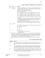
Writing b1 to a specific claim tag set bit sets that claim tag. Writing b0 to a specific claim tag
bit has no effect. This register always reads
0xFF
, indicating eight claim tags are implemented.
Claim Tag Clear Register
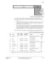
Figure 11-16 on page 11-33 shows the bit arrangement of the Claim Tag Set Register.
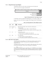
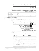
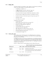
Figure 11-17 Claim Tag Clear Register format
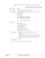
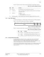
Table 11-28 shows how the bit values correspond with the Claim Tag Clear Register functions.
Writing b1 to a specific claim tag clear bit clears that claim tag. Writing b0 has no effect.
Reading this register returns the current claim tag value.
11.5.3
Lock Access Register
The Lock Access Register is a write-only register that controls writes to the debug registers. The
purpose of the Lock Access Register is to reduce the risk of accidental corruption to the contents
of the debug registers. It does not prevent all accidental or malicious damage. Because the state
of the Lock Access Register is in the debug power domain, it is not lost when the processor
powers down.
The Lock Access Register, bits [31:0] contain a key which controls the lock status. To unlock
the debug registers, write a
0xC5ACCE55
key to this register. To lock the debug registers, write any
other value. Accesses to locked debug registers are ignored. The lock is set on reset.
11.5.4
Lock Status Register
The Lock Status Register is a read-only register that returns the current lock status of the debug
registers.
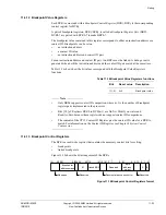
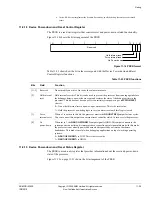
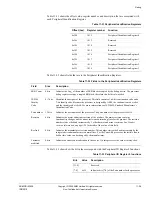
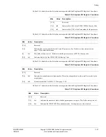
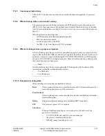
Figure 11-18 shows the bit arrangement of the Lock Status Register.
Figure 11-18 Lock Status Register format
31
0
Reserved
7
8
Claim tag clear
Table 11-28 Functional bits of the Claim Tag Clear Register
Bit
Field
Description
[31:8]
Reserved
RAZ or SBZP.
[7:0]
Claim tag clear
R/W. Reset value is
0x00
.
31
31
0
Reserved
1
2
3
32-bit access
Locked bit
Lock implemented bit

