Cycle Timings and Interlock Behavior
ARM DDI 0363E
Copyright © 2009 ARM Limited. All rights reserved.
14-21
ID013010
Non-Confidential, Unrestricted Access
14.13 Load and Store Multiple instructions
This section describes the cycle timing behavior for the
LDM
,
STM
,
PUSH
, and
POP
instructions.
These instructions take multiple cycles to issue, and then use multiple memory cycles to load
and store all the registers. Because the memory datapath is 64-bits wide, two registers can be
loaded or stored on each cycle.
This section describes:
•
Load and Store Multiples, other than load multiples including the PC
•
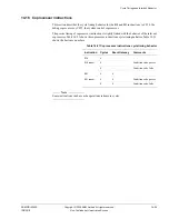
Load Multiples, where the PC is in the register list
on page 14-22
•
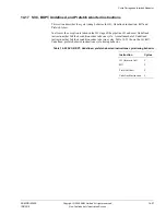
Example Interlocks
on page 14-22
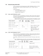
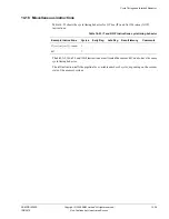
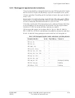
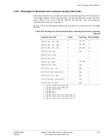
14.13.1 Load and Store Multiples, other than load multiples including the PC
In all cases the base register,
<Rn>
, is a Very Early Reg.
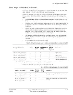
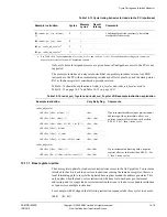
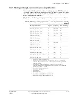
Table 14-17 shows the cycle timing behavior of load and store multiples including the PC.
Note
The Cycle timing behavior that Table 14-17 shows also covers
PUSH
and
POP
instructions that
behave like store and load multiple instructions with base register write-back.
Table 14-17 Cycle timing behavior of Load and Store Multiples, other than load multiples including the PC
Example instruction
Cycles
Cycles
with base
register
write-back
Memory
cycles
Result latency
(LDM)
Result latency
(base register)
First address 64-bit aligned
LDMIA <Rn>,{R1}
1
1
1
2
1
LDMIA <Rn>,{R1,R2}
1
2
1
2,2
2
LDMIA <Rn>,{R1,R2,R3}
2
2
2
2,2,3
2
LDMIA <Rn>,{R1,R2,R3,R4}
2
3
2
2,2,3,3
3
LDMIA <Rn>,{R1,R2,R3,R4,R5}
3
3
3
2,2,3,3,4
3
LDMIA <Rn>,{R1,R2,R3,R4,R5,R6}
3
4
3
2,2,3,3,4,4
4
LDMIA
<Rn>,{R1,R2,R3,R4,R5,R6,R7}
4
4
4
2,2,3,3,4,4,5
4
First address not 64-bit aligned
LDMIA <Rn>,{R1}
1
2
1
2
2
LDMIA <Rn>,{R1,R2}
2
2
2
2,3
2
LDMIA <Rn>,{R1,R2,R3}
2
3
2
2,3,3
3
LDMIA <Rn>,{R1,R2,R3,R4}
3
3
3
2,3,3,4
3
LDMIA <Rn>,{R1,R2,R3,R4,R5}
3
4
3
2,3,3,4,4
4
LDMIA <Rn>,{R1,R2,R3,R4,R5,R6}
4
4
4
2,3,3,4,4,5
4
LDMIA
<Rn>,{R1,R2,R3,R4,R5,R6,R7}
4
5
4
2,3,3,4,4,5,5
5

