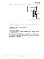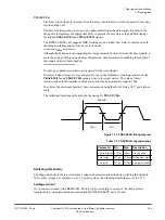
TCK
TDI
TMS
TDO
Debug unit
sets up TDI
and TMS
Target device
samples TDI
and TMS
Target
device sets
up TDO
Tclk
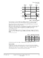
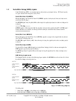
Figure 1-3 JTAG timing diagram
Since all signals are set up on the falling edge of
TCK
and sampled on the rising edge, the effective
setup and hold times for the target device and DSTREAM-PT system are approximately
Tclk
/2.
Issues with signal timing can usually be resolved by decreasing the
TCK
frequency. Decreasing the
TCK
frequency increases the setup and hold times.
TDO
is always slightly delayed, relative to the other signals, because it takes a finite amount of time for
the target device to detect the falling edge of
TCK
and then set up
TDO
. This slight delay, and the
round-trip delay of the debug cable, are compensated for by the DSTREAM-PT system.
Note
There are no separate timing requirements for the adaptive clocking mode. In adaptive clocking mode,
the debug unit samples
TDO
on the rising edge of
RTCK
instead of
TCK
, so
TDO
timing is relative to
RTCK
.
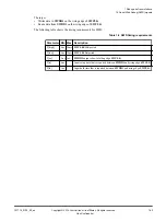
Table 1-1 JTAG timing Characteristics
Parameter Min
Max
Description
F[clk]
10Hz
180MHz
TCK
frequency
T[clk]
5.556ns 100ms
TCK
period
T[ds]
49%
51%
TCK
Duty Cycle
For further details on the JTAG interface, a full specification is available from:
.
Synchronization
As debug data is transferred to and from the target device, it must pass between two clock domains
(
TCK
and the internal system clock of the target device). To achieve synchronized data transfer without
suffering any meta-stability issues, a synchronizer circuit must be used within the target device.
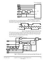
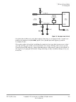
The following figure shows a circuit for a basic JTAG port synchronizer.
1 Debug and trace interface
1.1 JTAG signals
101714_0100_02_en
Copyright © 2019 Arm Limited or its affiliates. All rights reserved.
1-15
Non-Confidential


