nTRST
CLK
TCK
TDO
TMO
TDI
ASIC
nCLR
D
Q
D
Q
nCLR
RTCK
TDO
TCK
nTRST
CLK
TMS
TDI
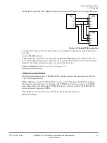
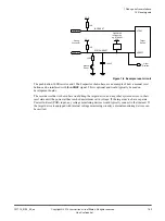
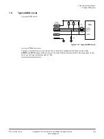
Figure 1-4 Basic JTAG port synchronizer
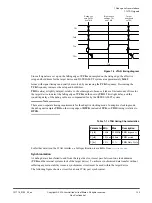
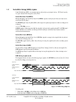
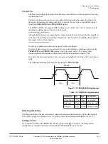
The following figure shows a partial timing diagram for the basic JTAG synchronizer. To reduce the
delay, and because the second flip-flop only provides better immunity to metastability problems, clock
the flip-flops from opposite edges of the system clock.
CLK
TCK
RTCK
Figure 1-5 Timing diagram for the Basic JTAG synchronizer
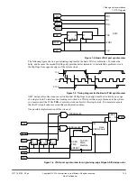
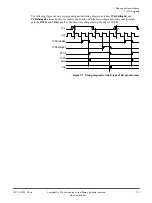
ASIC design rules often impose a restriction that all flip-flops in a design must be clocked by one edge
of a single clock. To interface the clocking restriction to a JTAG port that is asynchronous to the system,
you must convert the JTAG
TCK
events into clock enables for this single clock. You must also ensure
that the JTAG port cannot overrun this synchronization delay.
One possible implementation of this circuit, is:
CKEN
IN
nRESET
TMS
CKEN
TAP Ctrl
State
Machine
OUT
Scan
Chain
CKEN
TCKFalli ngEn
TCKRisingEn
Shift En
D
Q
nCLR
D
Q
nCLR
D
Q
nCLR
D
Q
TDO
TMS
CLK
nTRST
TCK
RTCK
TDI
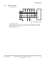
Figure 1-6 JTAG port synchronizer for single rising-edge D-type ASIC design rules
1 Debug and trace interface
1.1 JTAG signals
101714_0100_02_en
Copyright © 2019 Arm Limited or its affiliates. All rights reserved.
1-16
Non-Confidential

