1.8
I/O diagrams for DSTREAM-PT signals
The following diagrams and descriptions illustrate a simplified view of how each signal type is
connected within the debug unit.
Note
All comparator inputs have an indeterminate band of 100mV above, and below,
VTREF
/2. Signals that
are output from the target system, when passing through this voltage region, must be monotonic.
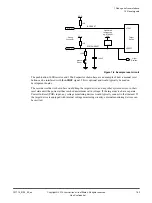
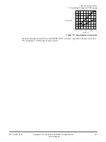
Input/Output signals
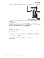
Standard input/output signals (
TDI
,
TMS
,
TDO
,
RTCK
,
SWDIO
,
DBGRQ
,
DBGACK
) use
LVCMOS
output buffers and comparator inputs with a series 33Ω resistor.
33R
VTREF/2
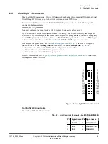
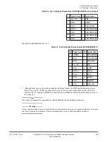
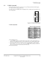
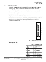
Figure 1-12 Input/Output signals
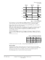
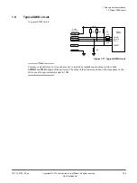
TCK signal
The
TCK
output signal is similar to a standard output signal, but also has a switchable capacitor, forming
a T-filter, which can reduce the
TCK
slew-rate.
Enabling this filter is not currently supported in Arm Development Studio.
16.5R
220pF
16.5R
Figure 1-13 TCK signal
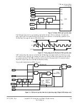
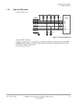
Reset signals
The reset signals (
nSRST
and
nTRST
) are similar to the standard input/output signals. However, they
have an extra LVCMOS driver, which is connected using a 4K7 resistor, that provides the weak pull-up
and pull-down functionality.
33R
4K7
VTREF/2
Strong Driver
Weak Driver
Figure 1-14 Reset signals
1 Debug and trace interface
1.8 I/O diagrams for DSTREAM-PT signals
101714_0100_02_en
Copyright © 2019 Arm Limited or its affiliates. All rights reserved.
1-28
Non-Confidential

