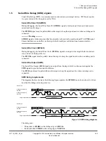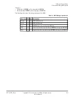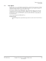
TRACECLK
The Trace Clock signal is an output from the target which is used to clock the parallel trace data
into the debug unit.
The trace clock signal does not need to be phase-shifted from the data signals. By default, the
debug unit incorporates the appropriate delay to provide the necessary setup and hold timings
for aligned
TRACEDATA
and
TRACECLK
signals.
The DSTREAM-ST only supports DDR clocking mode. Parallel trace data is captured on both
the rising and falling edges of the trace clock signal.
Note
Although the debug unit can compensate for large amounts of skew between the trace signals, to
avoid the extra calibration step during configuration, Arm recommends matching the lengths of
the signals within a 10mm window.
No pull-up or pull-down resistors are required for the trace signals.
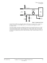
To improve signal integrity, it is good practice to provide impedance matching resistors on the
TRACEDATA
and
TRACECLK
outputs close to the target device. The value of these
resistors, added to the impedance of the driver, must be approximately equal to 50Ω.
To achieve the maximum data rate, Arm recommends using the short 20-way 0.05” pitch ribbon
cable.
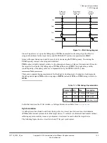
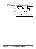
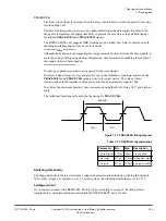
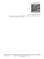
The following figure and table describe the timing for
TRACECLK
:
Tperiod
Twh
Twl
Figure 1-10 TRACECLK timing diagram
Table 1-3 TRACECLK characteristics
Parameter
Min
Max
Description
Tperiod (min) 1.667ns 125ms Clock period
Twh (min)
833ps
62.5ms High pulse width
Twl (min)
833ps
62.5ms Low pulse width
Switching thresholds
The debug unit detects the target reference voltage and automatically adjusts its switching thresholds to
50% of this voltage. For example, on a 3.3V target system, the switching thresholds are set to 1.65V.
Leakage current
If you connect an unpowered DSTREAM-ST unit to a powered target, on any of the debug or trace
signals, there is a maximum leakage current into the DSTREAM-ST unit of ±10μA.
1 Debug and trace interface
1.6 Trace signals
101714_0100_02_en
Copyright © 2019 Arm Limited or its affiliates. All rights reserved.
1-25
Non-Confidential


