Functional Description
ARM DDI 0275D
Copyright © 2002, 2003 ARM Limited. All rights reserved.
2-15
2.9
Trace RAM interface
This section describes the Trace RAM interface:
•
•
•
2.9.1
Signals
The TraceRAM interface block to the trace RAM uses the signals listed in Table 2-2.
The timing requirements for the ETB11 are described in Chapter 4
.
2.9.2
Read access
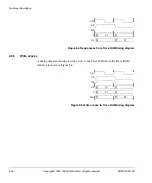
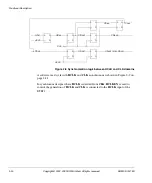
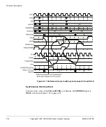
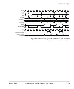
A timing diagram showing a read access from the Trace RAM to the Trace RAM
interface is shown in Figure 2-5 on page 2-16.
Table 2-2 Trace RAM interface signals
Signal
Description
CLK
Clock
A
A configurable width address bus
CE
An active HIGH chip enable signal
WE
An active HIGH write enable signal
D
RAM data input bus
OE
An active HIGH output enable signal
Q
RAM data output bus
Summary of Contents for ETB11
Page 6: ...List of Tables vi Copyright 2002 2003 ARM Limited All rights reserved ARM DDI 0275D ...
Page 8: ...List of Figures viii Copyright 2002 2003 ARM Limited All rights reserved ARM DDI 0275D ...
Page 46: ...Functional Description 2 26 Copyright 2002 2003 ARM Limited All rights reserved ARM DDI 0275D ...
Page 70: ...Signal Descriptions A 6 Copyright 2002 2003 ARM Limited All rights reserved ARM DDI 0275D ...
Page 78: ...Glossary Glossary 4 Copyright 2002 2003 ARM Limited All rights reserved ARM DDI 0275D ...

