Summary of Contents for MPS3

Page 1: ...Arm MPS3 FPGA Prototyping Board Technical Reference Manual Copyright 2017 2020 Arm Limited or its affiliates All rights reserved 100765_0000_04_en ...

Page 2: ...T NOT PROHIBITED BY LAW IN NO EVENT WILL ARM BE LIABLE FOR ANY DAMAGES INCLUDING WITHOUT LIMITATION ANY DIRECT INDIRECT SPECIAL INCIDENTAL PUNITIVE OR CONSEQUENTIAL DAMAGES HOWEVER CAUSED AND REGARDLESS OF THE THEORY OF LIABILITY ARISING OUT OF ANY USE OF THIS DOCUMENT EVEN IF ARM HAS BEEN ADVISED OF THE POSSIBILITY OF SUCH DAMAGES This document consists solely of commercial items You shall be res...

Page 3: ... arrange free collection when requested Recycle it using local WEEE recycling facilities These facilities are now very common and might provide free collection If purchased directly from Arm Arm provides free collection Please e mail weee arm com for instructions The CE Declaration of Conformity for this product is available on request The system should be powered down when not in use It is recomm...

Page 4: ... 17 2 2 Example Cortex M33 IoT Kit subsystem design 2 21 2 3 Clocks 2 23 2 4 Reset powerup and configuration 2 25 2 5 Power 2 27 2 6 Serial Configuration Controller interface 2 28 2 7 MCC SMC interface 2 30 2 8 USB 2 0 and Ethernet static memory interface 2 35 2 9 Video HDLCD interface 2 36 2 10 Audio codec interface 2 37 2 11 QVGA video CLCD display 2 38 2 12 On board user components 2 39 100765_...

Page 5: ... MCC command line interface 3 67 Appendix A Signal descriptions A 1 Debug connectors Appx A 71 A 2 Arduino Shield connectors Appx A 76 A 3 Peripheral Module Pmod connectors Appx A 80 A 4 FMC HPC connector Appx A 82 A 5 FMC configuration connector Appx A 83 A 6 Combined Ethernet and dual USB A connector Appx A 84 A 7 HDMI Type A female connector Appx A 85 A 8 Audio connectors stacked stereo jacks A...

Page 6: ...Arm MPS3 FPGA Prototyping Board Technical Reference Manual It contains the following About this book on page 7 Feedback on page 10 100765_0000_04_en Copyright 2017 2020 Arm Limited or its affiliates All rights reserved 6 Non Confidential ...

Page 7: ... is a list of terms used in Arm documentation together with definitions for those terms The Arm Glossary does not contain terms that are industry standard unless the Arm meaning differs from the generally accepted meaning See the Arm Glossary for more information Typographic conventions italic Introduces special terminology denotes cross references and citations bold Highlights interface elements ...

Page 8: ...serted signal depends on whether the signal is active HIGH or active LOW Asserted means HIGH for active HIGH signals LOW for active LOW signals Lowercase n At the start or end of a signal name n denotes an active LOW signal Additional reading This book contains information that is specific to this product See the following documents for other relevant information Arm publications Arm Cortex M Syst...

Page 9: ... website https www xilinx com for information about the Xilinx Kintex Ultrascale XCKU115 1FLVB1760C FPGA Preface About this book 100765_0000_04_en Copyright 2017 2020 Arm Limited or its affiliates All rights reserved 9 Non Confidential ...

Page 10: ...ata arm com Give The title Arm MPS3 FPGA Prototyping Board Technical Reference Manual The number 100765_0000_04_en If applicable the page number s to which your comments refer A concise explanation of your comments Arm also welcomes general suggestions for additions and improvements Note Arm tests the PDF only in Adobe Acrobat and Acrobat Reader and cannot guarantee the quality of the represented ...

Page 11: ...contains the following sections 1 1 Precautions on page 1 12 1 2 About the MPS3 board on page 1 13 1 3 Location of components on the MPS3 board on page 1 15 100765_0000_04_en Copyright 2017 2020 Arm Limited or its affiliates All rights reserved 1 11 Non Confidential ...
Page 12: ... board is intended for use within a laboratory or engineering development environment Caution To avoid damage to the MPS3 board observe the following precautions Connect the external power supply to the board before starting the powerup process Never subject the board to high electrostatic potentials Observe ElectroStatic Discharge ESD precautions when handling any board Always wear a grounding st...

Page 13: ...Versatile Express range Uses of the MPS3 board The MPS3 board enables FPGA prototyping of complex designs Software development Linux development on Cortex A or Cortex R class processors mbedOS Cortex Microcontroller Software Interface Standard CMSIS Real Time Operating System RTOS development on Cortex M class processors Bare metal development Tool development Major components and systems of the M...

Page 14: ...essor debug F JTAG FPGA debug Serial Wire Debug SWD 16 bit trace 4 bit trace On board CMSIS DAP Four serial ports over USB 1 Introduction 1 2 About the MPS3 board 100765_0000_04_en Copyright 2017 2020 Arm Limited or its affiliates All rights reserved 1 14 Non Confidential ...

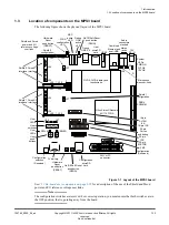
Page 15: ...ay and touchscreen 20 pin Cortex and debug 10 pin IDC 14 pin F JTAG ILA FPGA configuration LED Hardware Reset push button PBRST On Off Soft Reset push button PBON MCC active LED Debug USB active LED PWR ON 3V3 OK 12V OK System LEDs User LEDs PB1LED PB2LED Configuration switches Reserved J58 J59 Microphone bias user links L R Shield and Pmod power and I O reference voltage user links J24 J28 J34 J3...

Page 16: ...net static memory interface on page 2 35 2 9 Video HDLCD interface on page 2 36 2 10 Audio codec interface on page 2 37 2 11 QVGA video CLCD display on page 2 38 2 12 On board user components on page 2 39 2 13 Interrupts on page 2 40 2 14 FPGA DDR4 memory interface on page 2 41 2 15 User non volatile memory on page 2 42 2 16 Arduino Shield and Pmod interfaces on page 2 43 2 17 FMC HPC interface on...

Page 17: ...ipherals to enable FPGA prototyping and software development The following figure shows the hardware infrastructure of the MPS3 board 2 Hardware description 2 1 Overview of the board hardware 100765_0000_04_en Copyright 2017 2020 Arm Limited or its affiliates All rights reserved 2 17 Non Confidential ...

Page 18: ...face UART 4 UART CoreSight Trace connectors CoreSight CMSIS DAP controller ADC AD0 5 0 Shield 0 Pmod0 1 Pmod2 3 Shield 1 AD1 5 0 IO0 15 0 IO1 15 0 GPIO GPIO ADC controller F JTAG ILA F JTAG Hardware reset push buttons On Off Soft reset push buttons PBRST PBON Shield and Pmod expansion connectors MPS3 power supplies FMC HPC Board present Powerup board TLX User I O System LEDs Push button LEDs Figur...

Page 19: ...ver I2C from the I2C controller in the FPGA I2S audio connection to the I2S in the FPGA Shield expansion Two Arduino expansion interfaces for Shields for custom peripherals or off the shelf sensor interfaces such as WiFi Bluetooth Proximity detectors or Gyro sensors Each interface connects 16 digital 3V3 I O or 16 digital 5V I O voltage references and six analog inputs from each Shield Peripheral ...

Page 20: ... activity indicator incorporated into combined Ethernet and dual USB connector Related information 1 3 Location of components on the MPS3 board on page 1 15 2 Hardware description 2 1 Overview of the board hardware 100765_0000_04_en Copyright 2017 2020 Arm Limited or its affiliates All rights reserved 2 20 Non Confidential ...

Page 21: ... processors or dedicated customs designs The following figure shows an example Cortex M33 IoT Kit subsystem design for the MPS3 board You can implement this example design in MPS3 See Application Note AN524 Example SSE 200 Subsystem for MPS3 2 Hardware description 2 2 Example Cortex M33 IoT Kit subsystem design 100765_0000_04_en Copyright 2017 2020 Arm Limited or its affiliates All rights reserved...

Page 22: ...ripheral protection controller Default slave AHB5 GPIO Shields Pmod IDAU IDAU IDAU DMA DMA DMA SIE 200 System IP for Embedded CoreSight Trace connectors AHB5 exclusive access monitor AHB5 code interface AHB5 slave interface 0 AHB5 slave interface 1 Debug interfaces AHB5 master interface 0 AHB5 master interface 1 IoT kit AHB5 TrustZone master security controller AHB5 TrustZone master security contr...

Page 23: ...udio CODEC OSC0 Ethernet controller 25MHz OSC5 HDLCD HDMI controller MCC OSC 8MHZ DDR PHY OSC6 100MHz Fixed 32kHz 32 768kHz RTC MICTOR Cortex TCK CoreSight SMB DDR4 DDR CLK MCC Main Input Clock Configuration 25MHz CFG_CLK SCC OSCCLK 1 OSCCLK 2 OSCCLK 3 OSCCLK 4 OSCCLK 5 Figure 2 3 Overview of MPS3 board clocks The Motherboard Configuration Controller MCC configures the programmable OSCs at powerup...

Page 24: ...clock for the audio codec and FGPA audio interface In this case this clock is the source clock for AACI_MCLK AACI_SCLK AACI_LRCLK OSC0 25MHz default Ethernet controller 25MHz required by Ethernet controller OSC5 2 230MHz FPGA OSCCLK 5 The preferred use for this clock is for the HDMI controller and HDLCD interface in FPGA OSC6 100MHz default DDR PHY 100MHz required by DDR PHY OSC8MHz 8MHz fixed MCC...

Page 25: ...B_nRST FPGA_nRST SCC Debug nTRST CB_CFGnRST Fixed PSUs Fixed PSUs EN EN JTAG nSRST Reset logic GPIO MCC reset nRST Hardware reset push buttons On Off Soft reset push buttons PBRST PBON Figure 2 4 MPS3 board reset system FPGA resets FPGA_nRST Board and FPGA reset including FPGA PLLs CB_nPOR The main powerup reset for the FPGA image logic If a System Control Processor SCP is present in the design re...

Page 26: ... FPGA PLLs SCC config MCC reset PBON User ON CB_VRAMP FPGA_nRST CB_CFGnRST CB_nPOR CB_nRST CPUWAIT if supported nSRST Subsystem reset Release logic reset Release CPU reset Release processor wait Processor boot System running Warm reset Pre load memory Figure 2 5 MPS3 board reset and configuration timing Related information 1 3 Location of components on the MPS3 board on page 1 15 2 Hardware descri...

Page 27: ...e that it meets this criterion Alternatively you can connect an external 12V DC supply 10 directly to the 12V connector Caution Any external 12V DC 10 power supply that is used must be a limited power source maximum 5amps On board regulators supply power to the board power domains and to the FPGA power domains Note The following on board LEDs illuminate when power is applied 12V OK External 12V DC...

Page 28: ...FGDATAOUT Matrix Processor SMC Interrupt Configuration microSD Figure 2 6 Serial Configuration Controller interface Note If the design does not implement the SCC you must set the variable FPGA_SCC to FALSE in the board config txt file See 3 5 2 config txt generic board configuration file on page 3 64 The following figures show the read and write cycle timing of the SCC interface SCC reset Write ad...

Page 29: ...FGnRST CFGCLK A11 A10 A0 D31 D30 D0 Figure 2 8 Serial Configuration Controller interface write cycle timing 2 Hardware description 2 6 Serial Configuration Controller interface 100765_0000_04_en Copyright 2017 2020 Arm Limited or its affiliates All rights reserved 2 29 Non Confidential ...

Page 30: ... 0 SMBM_nOE SMBM_nWE SMBM_CLK SMBM_nWAIT Figure 2 9 MCC SMC interface Note SMBM_nBL 1 0 is not used The MCC SMC interface enables the MCC to access the peripheral space of the FPGA system Typical uses are Preloading boot images Reading and writing to system registers Preconfiguring peripherals Implementing the MCC SMC interface Chip Select SMBM_nE 4 1 functions as a Chip Select providing four acti...

Page 31: ...bytes and then the two most significant data bytes The following figure shows an MCC SMC interface address and data transfer SMBM_CLK READ WRITE ADDRESS READ WRITE DATA Two least significant bytes SMBM_nEx SMBM_A 25 16 SMBM_nWE SMBM_D 15 0 SMBM_nWAIT A 15 0 D 15 0 A 24 16 READ WRITE DATA Two most significant bytes D 31 16 Figure 2 10 MCC SMC interface address and data transfer timing Note The MCC ...

Page 32: ...l memory space of 256MB Each Chip Select can point to non contiguous areas in the user design But the total amount of user memory that each Chip Select accesses cannot exceed 64MB The six address bits generated by the design and if necessary the Chip Select bits define which parts of the user memory space are accessed The following figure shows the formation of the AHB 32 bit address in the FPGA 3...

Page 33: ...0 which gives a base address of 0x00000000 CS1 The image in the FPGA generates internal AHB address bits 31 26 0b000011 which gives a base address of 0x0C000000 CS2 The image in the FPGA generates internal AHB address bits 31 26 0b001100 which gives a base address of 0x30000000 CS3 The image in the FPGA generates internal AHB address bits 31 26 0b110000 which gives a base address of 0xC0000000 The...

Page 34: ...gn does not implement the MCC SMC interface you must set the variable FPGA_SMB to FALSE in the board config txt file See 3 5 2 config txt generic board configuration file on page 3 64 2 Hardware description 2 7 MCC SMC interface 100765_0000_04_en Copyright 2017 2020 Arm Limited or its affiliates All rights reserved 2 34 Non Confidential ...

Page 35: ... SMB_nOE SMB_nWE USB_nHCINT USB_DACK USB_DREQ ETH_INTR ETH_FIFOSEL OSC3A USB REF 12MHZ OSC4 ETH REF 25MHZ SMBF_CS 1 0 CS 1 CS 0 USB 2 0 Ethernet Combined Ethernet and dual USB 2 0 connector J2 Figure 2 13 MPS3 board USB 2 0 and Ethernet static memory interface Related information A 6 Combined Ethernet and dual USB A connector on page Appx A 84 1 3 Location of components on the MPS3 board on page 1...

Page 36: ... following figure shows a video HDLCD interface example design MPS3 FPGA Prototyping Board FPGA Processor Bus matrix HDLCD PLL OSC5 23 75MHz DDR4 Dynamic Memory Controller HDMI controller TDA 19988 24 bit RGB data synch and clock I2 S I2 C HDMI Figure 2 14 MPS3 board video HDLCD interface example design Related information A 7 HDMI Type A female connector on page Appx A 85 1 3 Location of componen...

Page 37: ...io codec drives the stacked stereo jack on the MPS3 board When using an electret type of microphones use jumpers J58 L and J59 R to enable microphone bias current The following figure shows an audio codec interface example design MPS3 FPGA Prototyping Board FPGA OSC5 24 576MHz Audio codec CS42L52 I2 S I2 C Mic In APB AACI_MCLK AACI_SCLK AACI_LRCLK AACI_SDIN AACI_SDOUT Line Out Line In Stacked ster...

Page 38: ...nal LCD_BLC connect to the GPIO interface in the FPGA The interface supports a screen update rate of 20fps The following figure shows a functional overview of the CLCD display system MPS3 FPGA Prototyping Board FPGA Dual I2 C LCD interface QVGA CLCD display panel with TSC Module MCBQVGA TS Controller HX8347 D I2C2_SCL I2C3_SCL I2C2_SDA I2C3_SDA LCD_DAT 17 10 LCD_RD LCD_WR LCD_RS LCD_CS LCD_TNC APB...

Page 39: ...igure shows the user components on the MPS3 board MPS3 FPGA Prototyping Board FPGA USER_SW 7 0 USER_LED 9 0 USER_PB 1 0 Switches GND PB1 PB2 1V8 LEDs Figure 2 17 MPS3 board user components Related information 1 3 Location of components on the MPS3 board on page 1 15 2 Hardware description 2 12 On board user components 100765_0000_04_en Copyright 2017 2020 Arm Limited or its affiliates All rights r...

Page 40: ...al interrupt signals that connect to external pins on the FPGA Table 2 2 Peripheral interrupts Interrupt Interrupt source IOFPGA_SYSWDT RTCC SYS_CFG OUT PB_IRQ Push button WDOG_RREQ Watchdog reset OUT DVI_INT HDMI interrupt USB_INT USB 2 0 ETH_INT Ethernet CLCD_TINT CLCD touchscreen 2 Hardware description 2 13 Interrupts 100765_0000_04_en Copyright 2017 2020 Arm Limited or its affiliates All right...

Page 41: ... 3 Byte Lane 4 Byte Lane 5 Byte Lane 6 Byte Lane 7 Byte Lane 8 Byte Lane 9 Byte Lane 10 Byte Lane 11 Byte Lane 12 I O I O I O I O I O I O I O I O I O I O I O I O I O bank 1 I O bank 2 I O bank 3 MIG DQ 63 0 DQS 7 0 DM 7 0 CS 1 0 BA 1 0 BG 1 0 ACT A 16 0 CKE 1 0 ODT 1 0 RESET PARIN ALERT 4GB DDR4 SODIMM MTA4ATF51264HZ 2G3B1 512MB Group 0 512MB Group 1 Bank 1 512MB Group 0 512MB Group 1 Bank 2 512MB...

Page 42: ...ssor NIC 400 microSD eMMC controller QSPI 8MB QSPI controller User microSD Dynamic Memory Controller Block RAM 8MB DDR4 4GB eMMC 16GB Port 1 Port 2 DAT 3 0 CLK CMD nCD DAT 7 0 CLK CMD nRST DS Figure 2 19 MPS3 board non volatile memory system example design Note The simplest boot method is to use block RAM in the FPGA which can be pre loaded by the MCC before resets are released The use of block RA...

Page 43: ...DC AD7490 ADC_CS ADC_CLK ADC_DIN ADC_DOUT IO1 15 0 AD0 5 0 AREF1 AD1 5 0 Shield 0 headers IO0 15 0 IO1 15 0 5V 3V3 IOREF0 IOREF1 VIN0 VIN1 Reset0 Reset1 System registers Level shifter 3V3 5V 12V Level shifter 3V3 5V 5V 3V3 5V 3V3 Pmod 0 Pmod 1 IOREF0 Pmod 2 Pmod 3 IOREF1 IOREF1 Pmod 0 header Pmod 1 header Shield 1 headers Pmod 2 header Pmod 3 header IOREF0 IOREF0 and VIN0 jumper connectors IOREF1 ...

Page 44: ...annels on each Shield Pmod interfaces The Pmod interfaces are an alternative to the Shield interfaces Each Pmod expansion header has 8 digital I O and supports the choice of 3V3 or 5V digital I O You can select the digital I O using two user links on the board One user link selects 3V3 or 5V digital I O operation for Pmod 0 and Pmod 1 The other user link selects 3V3 or 5V operation for Pmod 2 and ...

Page 45: ...for the Shield 1 interface Caution The maximum currents available at the power and reference pins are 3V3 IOREF 1A maximum available for both Shields and all four Pmod interfaces 5V IOREF 1A maximum available for both Shields and all four Pmod interfaces 12V 0 5A maximum available for both Shields See 1 3 Location of components on the MPS3 board on page 1 15 for the location of the user links Rela...

Page 46: ...ector MCC I2 C configuration FMC board configuration EEPROM I2 C DCC SPI Reserved for Arm daughterboards 10 MGTs 10 MGTs Figure 2 22 MPS3 board FMC HPC interface Note The FMC board configuration EEPROM is part of the FMC standard The Arm daughterboard configuration EEPROM and Daughterboard Configuration Controller DCC are not part of the FMC standard but are supplied with Arm FMC daughterboards FP...

Page 47: ...s revision history txt Application Note AN533 Blinky example FPGA image for the MPS3 Prototyping Board PDF document boardfiles Contains the FPGA image bit file and the MCC firmware ebf file that must be loaded onto the MPS3 microSD card to run the AN533 blinky design on the MPS3 board Example FMC board layout The following figure shows an MPS3 board with an FMC board that is fitted to the FMC HPC ...

Page 48: ...nfiguration of Arm FMC expansion boards The MPS3 board provides a custom 14 pin connector to enable configuration of Arm FMC boards using I2C SPI and reset signals The configuration process is similar to the configuration process used on the Arm Versatile Express boards that use the signals on the HDRY headers Arm FMC expansion boards provide a daughterboard EEPROM and a Daughterboard Configuratio...

Page 49: ... board AD9467 FMC Loopback board WHZ FMC XM 107 Related information A 4 FMC HPC connector on page Appx A 82 A 5 FMC configuration connector on page Appx A 83 1 3 Location of components on the MPS3 board on page 1 15 2 Hardware description 2 17 FMC HPC interface 100765_0000_04_en Copyright 2017 2020 Arm Limited or its affiliates All rights reserved 2 49 Non Confidential ...

Page 50: ...only CMSIS DAP Figure 2 24 MPS3 board CoreSight debug and trace P JTAG processor debug on 20 pin IDC connector 10 pin IDC connector 20 pin Cortex debug and ETM connector 38 pin MICTOR connector Serial Wire Debug SWD on 20 pin IDC connector 10 pin IDC connector 20 pin Cortex debug and ETM connector 38 pin MICTOR connector CMSIS DAP debug over USB on the Debug USB connector USB 2 0 type B connector ...

Page 51: ...s on the Kintex XCKU115 FPGA indicate the status of the system during boot time After the system has booted they are used for debug or status information The four serial ports are concentrated into a USB serial interface that connects to a four port hub that is connected to the USB connector The hub enables the four FPGA serial ports the MCC USBDBG port and the CMSIS DAP controller to share the US...

Page 52: ...C connector on page Appx A 72 A 1 3 20 pin Cortex debug and ETM connector on page Appx A 72 A 1 4 38 pin MICTOR connector on page Appx A 73 A 1 5 14 pin F JTAG ILA connector on page Appx A 74 A 1 6 Debug USB 2 0 connector on page Appx A 75 1 3 Location of components on the MPS3 board on page 1 15 2 Hardware description 2 18 System debug 100765_0000_04_en Copyright 2017 2020 Arm Limited or its affi...

Page 53: ...ie LOW QSPI_nCS Tie HIGH QSPI_SCLK Tie LOW IOFPGA_SYSWDT Tie LOW WDOG_RREQ Tie LOW SMBM_nWAIT Tie HIGH CFG_DATAOUT Tie LOW Configuration file settings If the design does not implement the Serial Configuration Controller SCC you must set the variable FPGA_SCC to FALSE in the board config txt file If the design does not implement the MCC SMC interface you must set the variable FPGA_SMB to FALSE in t...

Page 54: ...f the configuration system on page 3 55 3 2 Remote USB operation on page 3 57 3 3 Powerup and configuration sequence on page 3 58 3 4 Reset push buttons on page 3 61 3 5 Configuration files on page 3 63 3 6 MCC command line interface on page 3 67 100765_0000_04_en Copyright 2017 2020 Arm Limited or its affiliates All rights reserved 3 54 Non Confidential ...

Page 55: ...ou can access the configuration microSD card as a Universal Serial Bus Mass Storage Device USBMSD The MCC Reads the FPGA image from the configuration microSD card and loads it into the FPGA Sets the board oscillator frequencies using values from the MPS3 board configuration application note txt file If enabled configures the FPGA Serial Configuration Control SCC registers using values from the boa...

Page 56: ...vice with removable storage 2 The MCC loads the FPGA image into the FPGA Configuration port connected to an external workstation If you connect an external workstation to the MCC debug port you can access the configuration microSD card You can then edit and copy configuration and software images to the SD card Related information 3 5 1 Overview of configuration files and microSD card directory str...

Page 57: ...n reboot the system reset the system or shut down the system by using one of the following filenames reboot txt reset txt shutdown txt The MCC detects the presence of the files performs the requested command and deletes the file Note The contents of the files have no effect They can be empty files Related information 1 3 Location of components on the MPS3 board on page 1 15 A 1 6 Debug USB 2 0 con...

Page 58: ...e sequence of events of the board powerup and configuration process The following figure shows the powerup and configuration sequence 3 Configuration 3 3 Powerup and configuration sequence 100765_0000_04_en Copyright 2017 2020 Arm Limited or its affiliates All rights reserved 3 58 Non Confidential ...

Page 59: ... and does preliminary configuration Yes Resets CB_nPOR CB_nRST and CB_RUN released processor starts executing code On Off soft reset button pressed briefly Assert CB_nPOR CB_nRST and CB_RUN Hardware reset or On Off soft reset button pressed MCC reads generic config txt file from the configuration microSD card Configuration microSD card MB directory contains subdirectories that match the HBI code i...

Page 60: ...n files If the MCC finds configuration subdirectories that match the HBI code of the board configuration continues and the MCC reads the board txt file If the MCC does not find the correct configuration files it records the failure in a log file on the microSD card Configuration stops and the system re enters the standby state 8 The MCC measures the board power supplies 9 The MCC configures the bo...

Page 61: ...ST 2 The MCC asserts the CB_nRST signal The MCC might also assert CB_nPOR depending on the variable ASSERTNPOR in the configuration file config txt 3 The MCC releases CB_nPOR if it is active depending on the setting of the variable ASSERTNPOR in the configuration file config txt 4 The MCC releases CB_nRST 5 The board enters the run state Note The MCC does not perform the following actions as a res...

Page 62: ... a full configuration and enters the run state Related information 1 3 Location of components on the MPS3 board on page 1 15 3 Configuration 3 4 Reset push buttons 100765_0000_04_en Copyright 2017 2020 Arm Limited or its affiliates All rights reserved 3 62 Non Confidential ...

Page 63: ... the microSD card appears as a USB Mass Storage Device USBMSD You can then add edit or delete files You can use a standard text editor that produces DOS line endings to read and edit the board configuration files The following figure shows a typical example of the directory structure on the microSD card memory config txt LOG TXT V2MMPS3 F MB HBI0309B mbb_v ebf AN an _v bit an _v txt SOFTWARE st_v ...

Page 64: ...E Disable RTC UARTMODE 2 0 MCC FPGA0 1 MCC FPGA1 2 MCC FPGA0 FPGA1 REMAP BRAM Boot device BRAM DDR QSPI FPGA_SMB TRUE FPGA image supports the MCC SMB interface FPGA_SCC TRUE FPGA image supports the MCC SCC interface FMC_FORCE FALSE Force FMC power ON FMC_EEMODE 0 FMC EEPROM mode 0 default 1 two byte address DVIMODE VGA VGA SVGA XGA SXGA UXGA or HD1080 MCC sets OSC5 USERSWITCH 00000000 Userswitch 7...

Page 65: ...C0 25 0 Ethernet reference 25MHz 24 0 OSCCLK 0 refclk OSC1 32 0 OSCCLK 1 ACLK OSC2 50 0 OSCCLK 2 MCLK OSC3 50 0 OSCCLK 3 GPUCLK OSC4 24 576 OSCCLK 4 AUDCLK OSC5 23 75 0 OSCCLK 5 HDLCD MCC overrides this value OSC6 100 0 GTX clock DDR HARDWARE CONTROL ASSERTNPOR TRUE External resets assert nPOR LEGACYRST FALSE Legacy CB_nPOR CB_nRST reset mode CPUWAIT 0x00000002 CPUWAIT value set to 0xFFFFFFFF when...

Page 66: ...E st_emmc axf selftest emmc also supports QSPI boot IMAGE0DILE SOFTWARE demo_IoT axf V2M MSP3 demo IMAGE0FILE SOFTWARE shield axf Shield demo See 2 7 MCC SMC interface on page 2 30 for information on the IMAGE0ADDRESS variable axf and elf files are treated as elf files All other files are treated as binary Related information 3 1 Overview of the configuration system on page 3 55 3 3 Powerup and co...

Page 67: ... A Capture serial data to the file filename Use the A option to append data to an existing file Copy input_filename_1 input_filename_2 output_filename Copy file input_filename_1 to output_filename Option input_filename_2 merges input_filename_1 and input_filename_2 DEBUG Change to the debug menu DEL filename Delete file filename DIR mask Display a list of files in the directory EEPROM Change to th...

Page 68: ... system memory at address Note This command Is only ever available in run state Might not be available in your particular FPGA image 3 6 3 MCC debug menu To switch to the debug menu enter DEBUG at the MCC main menu The debug menu is valid only in the run state The following table shows the debug commands Table 3 2 MCC debug command menu Command Description CFG R W OSC V TEMP SCC device data Read W...

Page 69: ... Table 3 3 EEPROM commands Command Description CONFIG 0 filename Write configuration file to EEPROM EXIT or QUIT Return to main menu ERASECON 0 Erase configuration section of EEPROM ERASEDEV 0 Erase device section of EEPROM ERASERANGE 0 start end Erase EEPROM between start and end ERASEIMAGE image_id Erase image stored in board EEPROM ERASEIMAGES Erase images stored in board EEPROM HELP or Display...

Page 70: ...mod connectors on page Appx A 80 A 4 FMC HPC connector on page Appx A 82 A 5 FMC configuration connector on page Appx A 83 A 6 Combined Ethernet and dual USB A connector on page Appx A 84 A 7 HDMI Type A female connector on page Appx A 85 A 8 Audio connectors stacked stereo jacks on page Appx A 86 A 9 12V power connector on page Appx A 87 100765_0000_04_en Copyright 2017 2020 Arm Limited or its af...

Page 71: ...upports Serial Wire Debug SWD The 20 pin IDC connector connects to general purpose pins on the FPGA The availability of P JTAG or SWD depends on the design that you implement in the FPGA The following figure shows the 20 pin IDC connector J14 1 19 2 20 Figure A 1 20 pin IDC connector The following table shows the pin mapping for each P JTAG and SWD signal on the 20 pin IDC connector Table A 1 20 p...

Page 72: ...SWDCLK TCK 5 GND 6 SWO TDO 7 NC 8 NC TDI 9 GNDDETECT 10 nSRST Note Pins 2 6 8 and 10 have pullup resistors to 1V8 Pin 4 has a pulldown resistor to GND Related information 2 18 System debug on page 2 50 1 3 Location of components on the MPS3 board on page 1 15 A 1 3 20 pin Cortex debug and ETM connector The MPS3 board provides one 1V8 20 pin Cortex debug and Embedded Trace Macrocell ETM connector T...

Page 73: ...tion 2 18 System debug on page 2 50 1 3 Location of components on the MPS3 board on page 1 15 A 1 4 38 pin MICTOR connector The MPS3 board provides one 1V8 38 pin MICTOR connector The connector supports P JTAG processor debug to enable connection of DSTREAM or a compatible third party debugger The connector also supports Serial Wire Debug SWD and 16 bit trace The 38 pin MICTOR connector connects t...

Page 74: ...ETECT 33 TRACEDATA 10 34 1V8 reference 35 TRACEDATA 9 36 TRACECTL 37 TRACEDATA 8 38 TRACEDATA 0 Note Pins 9 11 17 19 and 21 have pullup resistors to 1V8 Pins 13 and 15 have pulldown resistors to GND Related information 2 18 System debug on page 2 50 1 3 Location of components on the MPS3 board on page 1 15 A 1 5 14 pin F JTAG ILA connector The MPS3 board provides one 3V3 14 pin F JTAG ILA connecto...

Page 75: ...bug on page 2 50 1 3 Location of components on the MPS3 board on page 1 15 A 1 6 Debug USB 2 0 connector The MPS3 board provides one USB 2 0 connector that supports configuration file editing in the microSD UART access to the FPGA and CMSIS DAP FPGA debug using SWD only The following figure shows the USB type B connector J8 Figure A 6 Debug USB 2 0 connector Related information 2 18 System debug o...

Page 76: ...H0 SH1_IO7 SH0 SH1_IO8 SH0 SH1_IO9 SH0 SH1_IO10 SH0 SH1_IO11 SH0 SH1_IO12 SH0 SH1_IO13 GND SH0 SH1_AREF SH0 SH1_IO14 SH0 SH1_IO15 SH0 SH1_AD5 SH0 SH1_AD4 SH0 SH1_AD3 SH0 SH1_AD2 SH0 SH1_AD1 SH0 SH1_AD0 SH0 SH1_VIN GND GND 5V 3V3 SH0 SH1_nRST SH0 SH1_IOREF N C SH0 SH1_nRST GND SH0 SH1_IO13 SH0 SH1_IO11 SH0 SH1_IO12 5V Connector J29 Shield interface 0 Connector J39 Shield interface 1 Connector J25 S...

Page 77: ... SH1_IO10 4 SH0 SH1_IO11 5 SH0 SH1_IO12 6 SH0 SH1_IO13 7 GND 8 SH0 SH1_AREF 9 SH0 SH1_IO14 10 SH0 SH1_IO15 Caution FPGA pins SH0_IO16 SH0IO17 SH1_IO16 and SH1_IO17 which are unused connect to the Shield connectors through 4K7 resistors FPGA pin SH0_IO16 connects to Shield pin SH0_IO14 FPGA pin SH0_IO17 connects to Shield pin SH0_IO15 FPGA pin SH1_IO16 connects to Shield pin SH1_IO14 FPGA pin SH1_I...

Page 78: ...references for Shield 0 digital I O Connector J35 provides power and voltage references for Shield 1 digital I O The following table shows the pin mapping for Shield connectors J26 and J35 Table A 9 Connectors J26 Shield 0 and J35 Shield 1 signal list Pin Signal 1 N C 2 SHO SH1_IOREF 3 SHO SH1_nRST 4 3V3 5 5V 6 GND 7 GND 8 SHO SH1_VIN Supplementary connectors J27 and J37 The supplementary connecto...

Page 79: ...IO11 5 SHO SH1_nRST 6 GND Related information 2 16 Arduino Shield and Pmod interfaces on page 2 43 1 3 Location of components on the MPS3 board on page 1 15 A Signal descriptions A 2 Arduino Shield connectors 100765_0000_04_en Copyright 2017 2020 Arm Limited or its affiliates All rights reserved Appx A 79 Non Confidential ...

Page 80: ...ins See 2 16 Arduino Shield and Pmod interfaces on page 2 43 for information on the user links and the maximum available IOREF current Caution The MPS3 board supports simultaneous use of Pmod and Shield expansion but you must exercise caution when driving the shared signals The following figure shows the Pmod connectors 1 7 12 6 Figure A 8 Pmod connectors J24 J28 J34 and J38 The following table sh...

Page 81: ...0_5V_IO13 10 SH1_5V_IO8 5 GND 11 GND 6 SH1_REF 12 SH1_REF The following table shows the pin mapping for the Pmod2 3 interface connector J38 Table A 14 Connectors J38 Pmod2 3 interface signal list Pin Signal Pin Signal 1 SH0_5V_IO3 7 SH1_5V_IO4 2 SH0_5V_IO9 8 SH1_5V_IO2 3 SH0_5V_IO0 9 SH1_5V_IO15 4 SH0_5V_IO1 10 SH1_5V_IO14 5 GND 11 GND 6 SH1_REF 12 SH1_REF Related information 2 16 Arduino Shield a...

Page 82: ...d ANSI VITA 57 1 See http www vita com for the pin mapping of the FMC HPC connector Arm supplies two spreadsheets that describe the FPGA FMC connectivity on the MPS3 board See FPGA FMC pin connectivity on page 2 46 for information on how to download the spreadsheets Related information 2 17 FMC HPC interface on page 2 46 1 3 Location of components on the MPS3 board on page 1 15 A Signal descriptio...

Page 83: ...ollowing figure shows the FMC HPC configuration connector J61 1 13 2 14 Figure A 10 FMC HPC configuration connector Related information 2 17 FMC HPC interface on page 2 46 1 3 Location of components on the MPS3 board on page 1 15 A Signal descriptions A 5 FMC configuration connector 100765_0000_04_en Copyright 2017 2020 Arm Limited or its affiliates All rights reserved Appx A 83 Non Confidential ...

Page 84: ...dual USB A connector J2 USB 2 0 port 1 USB 2 0 port 2 Ethernet 10 100 Figure A 11 Combined Ethernet and dual USB A connector Related information 2 8 USB 2 0 and Ethernet static memory interface on page 2 35 1 3 Location of components on the MPS3 board on page 1 15 A Signal descriptions A 6 Combined Ethernet and dual USB A connector 100765_0000_04_en Copyright 2017 2020 Arm Limited or its affiliate...

Page 85: ... HDMI connector J3 signal list Pin Signal Pin Signal 1 DVI_TX2P 2 GND 3 DVI_TX2N 4 DVI_TX1P 5 GND 6 DVI_TX1N 7 DVI_TX0P 8 GND 9 DVI_TX0N 10 DVI_TXCP 11 GND 12 DVI_TXCN 13 DVI_CECAO 14 No connection 15 DVI_DSCLO 16 DVI_DSDAO 17 GND 18 DVI_5V0 19 DVI_HPDO Related information 2 9 Video HDLCD interface on page 2 36 1 3 Location of components on the MPS3 board on page 1 15 A Signal descriptions A 7 HDM...

Page 86: ...s the microphone in connector When using electret microphones use jumpers J58 L and J59 R to enable microphone bias current The following figure shows the three stereo jack connectors J4 Line in Blue Line out Green Mic in Pink Figure A 13 Stacked stereo jack connectors Related information 2 10 Audio codec interface on page 2 37 1 3 Location of components on the MPS3 board on page 1 15 A Signal des...

Page 87: ...r jack Alternatively you can connect an external 12V 5A 10 power supply to the power jack Note The center pin is the positive side of the power supply Related information 2 5 Power on page 2 27 1 3 Location of components on the MPS3 board on page 1 15 A Signal descriptions A 9 12V power connector 100765_0000_04_en Copyright 2017 2020 Arm Limited or its affiliates All rights reserved Appx A 87 Non ...

Page 88: ...electrical specifications of the MPS3 board It contains the following section B 1 Available power for expansion boards on page Appx B 89 100765_0000_04_en Copyright 2017 2020 Arm Limited or its affiliates All rights reserved Appx B 88 Non Confidential ...

Page 89: ...fitted The following table shows the maximum current that the board can supply from each power rail Table B 2 Shield and Pmod power Power rail Max load Comment 3V3 1A Maximum current available for both Shields or all four Pmod expansion boards Includes digital I O reference IOREF 5V 1A Maximum current available for both Shields or all four Pmod expansion boards Includes digital I O reference IOREF...

Page 90: ...bes the technical changes between released issues of this book It contains the following section C 1 Revisions on page Appx C 91 100765_0000_04_en Copyright 2017 2020 Arm Limited or its affiliates All rights reserved Appx C 90 Non Confidential ...

Page 91: ...formation about remote USB operation 3 2 Remote USB operation on page 3 57 2 18 System debug on page 2 50 All versions Updated example configuration application note txt file 3 5 3 Contents of the MB directory on page 3 64 All versions Added information about command line interface 3 6 MCC command line interface on page 3 67 All versions Table C 4 Differences between issue 100765_0000_02 and issue...

Page 92: ...1 Added information about Application Note AN533 download Download includes detailed information about FPGA FMC pin connectivity FPGA FMC pin connectivity on page 2 46 All versions Added link to section FPGA FMC pin connectivity on page 2 46 in FMC HPC connector description A 4 FMC HPC connector on page Appx A 82 All versions Added Application Note AN533 Blinky example FPGA image for the MPS3 Prot...

Reviews: