2.11
QVGA video CLCD display
The MPS3 board provides QVGA, 320 × 240, CLCD video display.
The CLCD video display system provides an on
‑
board CLCD display panel that includes:
• An 8
‑
bit parallel bus between the FPGA and the display panel.
• A 4
‑
wire resistive touch screen.
• A
Touch Screen Controller
(TSC) that connects to the FPGA over an I
2
C bus.
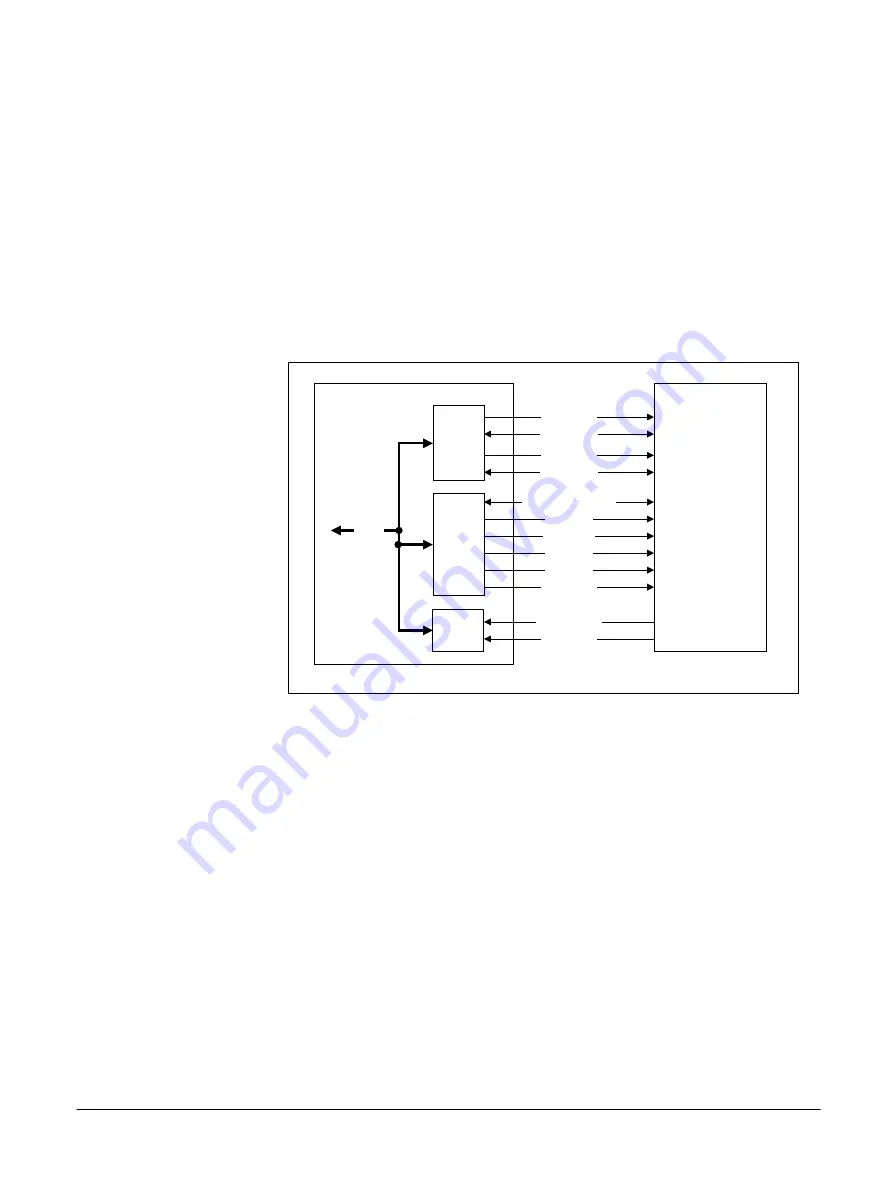
The interrupt signal from the touch screen controller,
LCD_TSINT
, and the backlight control signal,
LCD_BLC
, connect to the GPIO interface in the FPGA.
The interface supports a screen update rate of 20fps.
The following figure shows a functional overview of the CLCD display system.
MPS3 FPGA Prototyping Board
FPGA
Dual I
2
C
LCD
interface
QVGA CLCD
display panel with
TSC
Module
MCBQVGA-TS
Controller
HX8347-D
I2C2_SCL
I2C3_SCL
I2C2_SDA
I2C3_SDA
LCD_DAT[17:10]
LCD_RD
LCD_WR
LCD_RS
LCD_CS
LCD_TNC
APB
GPIO
LCD_TSINT
LCD_BLC
Figure 2-16 MPS3 board CLCD display system
2 Hardware description
2.11 QVGA video CLCD display
100765_0000_04_en
Copyright © 2017–2020 Arm Limited or its affiliates. All rights
reserved.
2-38
Non-Confidential


