background image

Chapter 3

MVME8100 / MVME8110 Installation and Use (6806800P25J)

59

Connectors, LEDs, and Switches

This chapter summarizes the Front Panel Connectors, LEDs, and On-Board Switches and their 
configuration for the MVME8100 /MVME8110 board.

The following components are found on MVME8100 / MVME8110 front panel. Refer to 

Figure 

3-1

 for the location of each component.

Figure 3-1

ENP1 Board Connectors, LEDs, Switches

Console Port 
Micro-DB9 

Reset Switch 


USB  

2.0 

Activity LED


Link LED


Board

 Fail LED


User


LED


Gigabit Ethernet 

Port 

Summary of Contents for MVME8100

Page 1: ...MVME8100 MVME8110 Installation and Use P N 6806800P25J August 2015 ...

Page 2: ...hanges from time to time in the content hereof without obligation of Artesyn to notify any person of such revision or changes Electronic versions of this material may be read online downloaded for personal use or referenced in another document as a URL to an Artesyn website The text itself may not be published commercially in print or electronic form edited translated or otherwise altered without ...

Page 3: ...1 Unpacking and Inspecting the Board 40 2 2 Requirements 41 2 2 1 Environmental Requirements 41 2 2 2 Power Requirements 43 2 2 3 Thermal Requirements 44 2 2 4 Thermally Significant Components 44 2 2 5 Equipment Requirements 44 2 3 Configuring the Board 44 2 4 Installing Accessories 46 2 4 1 Rear Transition Module 47 2 4 2 PMC XMC Installation 48 2 4 3 SATA Installation 51 2 5 Installing and Remov...

Page 4: ...3 3 1 5 Reset Abort Switch 83 4 Functional Description 85 4 1 Block Diagram 86 4 2 Processor 88 4 3 System Memory 88 4 4 Timers 88 4 4 1 Real Time Clock 89 4 4 2 P5020 P5010 Internal Timers 89 4 4 3 Watchdog Timers 89 4 4 3 1 Initial Hardware Watchdog 90 4 4 3 2 OS Watchdog 90 4 4 4 CPLD Tick Timer 90 4 5 Ethernet Interfaces 90 4 6 SPI Interface 91 4 6 1 SPI Flash Memory 91 4 6 2 Firmware Redundan...

Page 5: ...ower Sequence Requirements 101 4 20 Clock Structure 102 4 21 Reset Structure 103 4 22 Interrupt Controller Assignments 105 4 23 GPIO Electrical Characteristics 106 4 24 Thermal Management 106 5 Boot System 109 5 1 Accessing U Boot 109 5 2 Boot Options 110 5 2 1 Booting from a Network 110 5 2 2 Booting from an Optional SATA Drive 111 5 2 3 Booting from a USB Drive 111 5 2 4 Booting from eMMC 112 5 ...

Page 6: ...stallation and Use 6806800P25J Contents 6 Contents Contents B Related Documentation 119 B 1 Artesyn Embedded Technologies Embedded Computing Documentation 119 B 2 Related Specifications 119 B 3 Manufacturers Documents 121 ...

Page 7: ...able 3 9 PMC J12 J22 Connector 70 Table 3 10 PMC J13 J23 Connectors 72 Table 3 11 PMC J14 Connector 73 Table 3 12 Asset JTAG Header Pin Assignment P12 75 Table 3 13 XMC Connectors 75 Table 3 14 Front Panel LEDs 77 Table 3 15 On board LEDs Status 78 Table 3 16 S2 Switch Settings 79 Table 3 17 S3 Switch Settings 80 Table 3 18 Three Row Backplane Manual Slot Addressing 81 Table 3 19 S4 Switch Setting...

Page 8: ...MVME8100 MVME8110 Installation and Use 6806800P25J 8 List of Tables ...

Page 9: ...a PMC XMC Module on a VME Module 51 Figure 2 4 SATA drive Installation 53 Figure 3 1 ENP1 Board Connectors LEDs Switches 59 Figure 3 2 ENP4 LEDs and Switches 60 Figure 4 1 Block Diagram of MVME8100 86 Figure 4 2 Block Diagram of MVME8110 87 Figure 4 3 PCIe Ports 94 Figure 4 4 SRIO Bus Topology 95 Figure 4 5 I2C Busses 99 Figure 4 6 Power Distribution 101 Figure 4 7 Clock Structure 102 Figure 4 8 R...

Page 10: ...MVME8100 MVME8110 Installation and Use 6806800P25J 10 List of Figures ...

Page 11: ...herheitshinweise is a German translation of the Safety Notes chapter Chapter 1 Introduction gives an overview of the features of the product standard compliances mechanical data and ordering information Chapter 2 Hardware Preparation and Installation outlines the installation requirements hardware accessories switch settings and installation procedures Chapter 3 Connectors LEDs and Switches descri...

Page 12: ...C Error Correction Code EEPROM Electrically Erasable Programmable Read Only Memory eMMC Enhanced Module Management Controller FCC Federal Communications Commission FIFO First In First Out GMII Gigabit Media Independent Interface IEEE Institute of Electrical and Electronics Engineers I2C Inter IC IWD Initial Hardware Watchdog JTAG Joint Test Access Group LBC Local Bus Controller MRAM Magnetoresisti...

Page 13: ...nt SBC Single Board Computer SDRAM Synchronous Dynamic Random Access Memory SELV Safety Extra Low Voltage SMT Surface Mount Technology SGMII Serial Gigabit Media Independent Interface SPD Serial Presence Detect SRAM Static Random Access Memory SRIO Serial Rapid IO TSEC Three Speed Ethernet Controller 2eSST Two edge Source Synchronous Transfer UART Universal Asynchronous Receiver Transmitter VITA V...

Page 14: ...dforon screenoutputandcoderelatedelements or commands in body text Courier Bold Used to characterize user input and to separate it from system output Reference Used for references and for table and figure descriptions File Exit Notation for selecting a submenu text Notation for variables and keys text Notation for software buttons to click on the screen and parameter description Repeated item for ...

Page 15: ...ge No danger encountered Pay attention to important information Notation Description Part Number Publication Date Description 6806800P25A May 2012 First edition 6806800P25B November 2012 GA release 6806800P25C December 2012 Updated Standard Compliances on page 34 6806800P25D September 2013 Updated Table 1 1 Table 1 2 Table 2 1 Table 2 3 PMC XMC Installation on page 48 Table 3 2 on page 61 and Tabl...

Page 16: ... Boot System 6806800P25F June 2014 Re branded to Artesyn template 6806800P25G September 2014 Changed title as MVME8100 MVME8110 Added information about MVME8110 and Declaration of Conformity 6806800P25H October 2014 Updated Boot Options 6806800P25J July 2015 Updated CPLD Tick Timer section Part Number Publication Date Description ...

Page 17: ...tion Only personnel trained by Artesyn Embedded Technologies or persons qualified in electronics or electrical engineering are authorized to install remove or maintain the product The information given in this manual is meant to complete the knowledge of a specialist and must not be used as replacement for qualified personnel Keep away from live circuits inside the equipment Operating personnel mu...

Page 18: ...requency emissions compliance is maintained Operation Product Damage High humidity and condensation on the board surface causes short circuits Do not operate the board outside the specified environmental limits Make sure the board is completely dry and there is no moisture on any surface before applying power Damage of Circuits Electrostatic discharge and incorrect installation and removal can dam...

Page 19: ...unction Product Damage Inserting or removing modules with power applied may result in damage to module components Before installing or removing additional devices or modules read the documentation that came with the product Cabling and Connectors Product Damage RJ 45 connectors on modules are either twisted pair Ethernet TPE or E1 T1 J1 network interfaces Connecting an E1 T1 J1 line to an Ethernet...

Page 20: ...esentative for the availability of alternative officially approved battery models Data Loss Exchanging the battery can result in loss of time settings Backup power prevents the loss of data during exchange Quickly replacing the battery may save time settings Data Loss If the battery has low or insufficient power the RTC is initialized Exchange the battery before seven years of actual battery use h...

Page 21: ... Geschäftsstelle von Artesyn Embedded Technologies Das Produkt wurde entwickelt um die Sicherheitsanforderungen für SELV Geräte nach der Norm EN 60950 1 für informationstechnische Einrichtungen zu erfüllen Die Verwendung des Produkts in einer anderen Anwendung erfordert eine Sicherheitsüberprüfung für diese spezifische Anwendung Einbau Wartung und Betrieb dürfen nur von durch Artesyn Embedded Tech...

Page 22: ...ies durchgeführt werden können dazu führen dass der Anwender die Genehmigung zum Betrieb des Produktes verliert Boardprodukte werden in einem repräsentativen System getestet um zu zeigen dass das Board den oben aufgeführten EMV Richtlinien entspricht Eine ordnungsgemässe Installation in einem System welches die EMV Richtlinien erfüllt stellt sicher dass das Produkt gemäss den EMV Richtlinien betri...

Page 23: ...as Produkt installieren Installation Datenverlust Das Herunterfahren oder die Deinstallation eines Boards bevor das Betriebssystem oder andere auf dem Board laufende Software ordnungsmemäss beendet wurde kann zu partiellem Datenverlust sowie zu Schäden am Filesystem führen Stellen Sie sicher dass sämtliche Software auf dem Board ordnungsgemäss beendet wurde bevor Sie das Board herunterfahren oder ...

Page 24: ... verbundenen TPE Kabels 100 m nicht überschreitet Das Produkt darf über die TPE Stecker nur mit einem Sicherheits Kleinspannungs Stromkreis SELV verbunden werden Bei Fragen wenden Sie sich an Ihren Systemverwalter Batterie Beschädigung des Blades Ein unsachgemäßer Einbau der Batterie kann gefährliche Explosionen und Beschädigungen des Blades zur Folge haben Verwenden Sie deshalb nur den Batteriety...

Page 25: ...utzung vergangen sind Schäden an der Platine oder dem Batteriehalter Wenn Sie die Batterie mit einem Schraubendreher entfernen können die Platine oder der Batteriehalter beschädigt werden Um Schäden zu vermeiden sollten Sie keinen Schraubendreher zum Ausbau der Batterie verwenden Umweltschutz Entsorgen Sie alte Batterien und oder Blades Systemkomponenten RTMs stets gemäß der in Ihrem Land gültigen...

Page 26: ...MVME8100 MVME8110 Installation and Use 6806800P25J Sicherheitshinweise 26 ...

Page 27: ... reduced version of the VXS1 RTM1 1 1 Features The main features of the MVME8100 board are as follows Processor Subset of P5020 features used on MVME8100 Freescale QorIQ P5020 Two e5500 Power Architecture cores Five Gigabit Ethernet controllers Serial Gigabit Media Independent Interface SGMII and Reduced Gigabit Media Independent Interface RGMII interfaces Two 64 bit DDR3 3L SDRAM memory controlle...

Page 28: ...C with battery backup Temperature Sensors RTM and XMC VPD EERPOMs FLASH Two soldered SPI FLASH 8MB each switchable for uboot primary backup support Hardware switch or Software bit write protection for entire logical bank Eight GB eMMC Flash NVRAM 512 KB MRAM PCI Express Two 4X Ports to VXS backplane P0 muxed with SRIO ports One 8X Port to PMC XMC Site 1 One 4X Port to PMC XMC Site 2 SRIO Two 4X Po...

Page 29: ...nd 2eSST Timers Eight 32 bit timers in CPU Watchdog timer in CPU PMC XMC Two PMC XMC sites with 64 bit PMCIO on Site 1 Serial AT Attachment SATA SSD Option for one 2 5 inch SATA drive PMC XMC Site 2 GPIO Interface Two GPIOs to RTM VXS Interface VXS VITA 41 Specification compliant Support backplane P0 connector Form Factor Standard 6U one slot Support 0 8 and 0 85 inch slot chassis Support heat fra...

Page 30: ...s Two 10 100 1000BASE T Ethernet channels to RJ45 connectors on RTM panel Two 1000 BASE BX Ethernet SERDES channels to backplane Two USB2 0 ports to RTM with USB type A connectors on RTM panel One SATA port to RTM with eSATA connector on RTM Two GPIOs to planar headers on RTM Note The front panel I O connectors are available only in ENP1 air cooled variants I O signals in ENP4 conduction cooled va...

Page 31: ...Dual UART RAID5 6 engine SEC not present Programmable interrupt controller System Memory Up to 4GB Single Channel DDR3 1333 memory with ECC SM Bus One 512 Kbit user configuration serial EEPROM 256B SPD EEPROMs One 64 Kbit VPD EEPROM RTC with battery backup Temperature Sensors RTM and XMC VPD EERPOMs FLASH Two soldered SPI FLASH 8MB each switchable for uboot primary backup support Hardware switch o...

Page 32: ...Ports One RS232 422 485 console port to front panel Up to 4 RS232 422 485 COM ports to P2 RTM VME Bus VME64x and 2eSST Timers Eight 32 bit timers in CPU Watchdog timer in CPU PMC XMC Two PMC XMC sites with 64 bit PMCIO on Site 1 SATA SSD Option for one 2 5 inch SATA drive PMC XMC Site 2 GPIO Interface Two GPIOs to RTM Form Factor Standard 6U one slot Support 0 8 and 0 85 inch slot chassis Support ...

Page 33: ...e front panel RJ45 connector with integrated LEDs for 10 100 1000 Ethernet channel PMC XMC site 1 front I O and rear PMC I O PMC XMC site two front I O Four Serial ports to P2 RTM two with micro DB9 connectors on RTM panel and two on planar headers Two 10 100 1000BASE T Ethernet channels to RJ45 connectors on RTM panel Two 1000 BASE BX Ethernet SERDES channels to backplane Two USB2 0 ports to RTM ...

Page 34: ...0950 1 Safety Requirements legal CISPR 22 EN 55022 EN 55024 FCC Class A VCCI Japan AS NZS CISPR 22 EMC requirements legal on system level predefined Artesyn Embedded Technologies system ETSI EN 300 019 series Environmental Requirements Directive 2002 95 EC Directive on the restriction of the use of certain hazardous substances in electrical and electronic equipment RoHS The ENP1 version complies w...

Page 35: ... of 2004 108 EC 2006 95 EC 2011 65 EU and their amending directives Product MVME8100 Series VMEbus Single Board Computer Model Name Number MVME8100 202180404 MVME8100 202200401E MVME8100 202200401S MVME8100 202200404 has been designed and manufactured to the following specifications EN55022 2010 EN55024 2010 IEC 60950 1 2005 2nd Edition EN60950 1 2006 A11 2009 2011 65 EU RoHS Directive As manufact...

Page 36: ...ng product in accordance with the requirements of 2004 108 EC 2011 65 EU and their amending directives Product MVME8110 Series VMEbus Single Board Computer Model Name Number MVME8110 01E MVME8110 01S MVME8110 RTM has been designed and manufactured to the following specifications EN55022 2010 EN55024 2010 Edition 2 2011 65 EU RoHS Directive As manufacturer we hereby declare that the product named a...

Page 37: ... following tables 1 4 1 Supported Board Models Table 1 2 Mechanical Data Characteristic Value Height 233 44 mm 9 2inches Depth 160 0 mm 6 3 inches Front Panel Height 261 8 mm 10 3 inches Width 19 8 mm 0 8 inches Maximum Component Height 14 8 mm 0 58 inches Weight estimated 0 58 Kg ENP1 0 90 Kg ENP4 Table 1 3 Board Variants Marketing Processor MVME8100 202200401E P5020 2 0GHz 28W 4GB DDR3 VXS 2 PMC...

Page 38: ...110 MVME8110 01S P5010 1 2GHZ 2GB DDR3 2PMC XMC ENP1 SCANBE Table 1 3 Board Variants continued Marketing Processor Model Number Description VXS1 RTM1 RTM for MVME8100 supports ENP1 specifications only MVME8100 HDMTKIT4 SSD Mounting kit HDD not included MVME8110 RTM RTM FOR THE MVME8110 MVME8100 HDMTKIT4 CC MVME8100 HARD DRIVE MOUNTING KIT ENP1 AND 4 CONF COAT HDD not included ...

Page 39: ...ad the entire chapter including all caution and warning notes before you begin 1 Unpack the hardware Unpacking and Inspecting the Board on page 40 2 Configure the hardware by setting jumpers on the board and RTM Configuring the Board on page 44 3 Install the RTM VXS1 RTM1 of MVME8100 or MVME8110 RTM of MVME8110 in the chassis Rear Transition Module on page 47 4 Install PMC module if required Insta...

Page 40: ...ms ordered 2 Check for damage and report any damage or differences to customer service 3 Remove the desiccant bag shipped together with the board and dispose of it according to your country s legislation Damage of Circuits Electrostatic discharge and incorrect installation and removal can damage circuits or shorten their life Before touching the board or electronic components make sure that you ar...

Page 41: ...seboard appears in Chapter 4 Functional Description The MVME8100 has ENP1 and ENP4 variants which comply with the following environmental and regulatory specifications The MVME8110 has ENP1variant only which comply with the following environmental and regulatory specifications For ENP1 boards the operating temperatures refer to the temperature of the air circulating around the board and not to the...

Page 42: ... while supported by other components on the board may result in an unspecified reduction in the data retention capabilities of the eMMC Relative humidity To 95 RH To 100 RH Vibration Sine 10min axis 2G 5 to 500 Hz 10G 15 to 2000 Hz Vibration Random 1hr axis 0 002g2 Hz 15 to 2000 Hz1 2G RMS 0 1g2 Hz 15 to 2000 Hz 12GRMS 2 Shock 20g 11mS 40g 11mS Conformal Coating No Option Acrylic Product Damage Hi...

Page 43: ...le shows the power limits due to the available 5 volts pins when the MVME8100 is installed in either a 3 row or 5 row chassis and when PMCs XMCs are present Table 2 2 Operating Voltages Voltages Minimum Normal Maximum 5 0 V 4 875 V 2 5 5 0 V 5 25 V 5 Table 2 3 Power Requirements Board Variant Power MVME8100 202200401S E MVME8110 01S E ENP1 Board idle at OS prompt 38 Watts typical Operating load 42...

Page 44: ... that the processor core temperature does not exceed 100 C The processor core temperature can be read using the I2Csensorataddress0x4ContheprocessorI2Cbus 1 Formoreinformation referMVME8100 MVME8110 Single Board Computer Programmer s Reference 2 2 5 Equipment Requirements The following equipment is recommended to complete an MVME8100 MVME8110 system VMEbus system enclosure System console terminal ...

Page 45: ...110 baseboard ensure that all switches that are user configurable are set properly To do this refer to Figure 2 1 or the board itself for the location of specific switches and set the switches according to the descriptions provided in Configuration Switches on page 79 Figure 2 1 Switch Locations ENP1 board S5 Switch S2 Switch S3 Switch S4 Switch ...

Page 46: ...10 Installation and Use 6806800P25J 46 2 4 Installing Accessories ThissectiondescribestheproceduresforinstallingtheRTMofMVME8100 MVME8110 PMCs and the XMCspan on the baseboard Figure 2 2 Switch Locations ENP4 Board S5 Switch S4 Switch S2 Switch S3 Switch ...

Page 47: ... rear card cage 4 Install the top and bottom edge of the RTM into the rear guides of the chassis 5 Ensure that the levers of the two injector ejectors are in the outward position Damage of Circuits Electrostatic discharge and incorrect installation and removal can damage circuits or shorten their life Before touching the board or electronic components make sure that you are working in an ESD safe ...

Page 48: ...vent pin damage 6 Remove the transition module from the chassis and insert the filler panels 2 4 2 PMC XMC Installation The PMC connectors are placed to support two single width PMCs or one double width PMC PMC site 1 supports front PMC I O and rear PMC I O via the Jn4 connector PMC 1 I O is routed to the VME P2 connector PMC site 2 only supports front PMC I O and does not have a Jn4 connector The...

Page 49: ...iththeboardwhentheconnectorsonthe module align with the mating connectors on the board Note ENP4 PMC XMC modules do not have front bezels Logic Ground to Chassis Ground Isolation The MVME8100 MVME8110 heat frames are isolated from the board logic ground Installing a PMC or XMC module which has mounting locations connected to the module logic ground will result in a short between chassis ground and...

Page 50: ...sert the two front PMC XMC mounting screws through the mounting holes on the bottom side of the board and then install the top side screws Tighten the screws Note RuggedPMC XMCmodulesinstalledonanENP4MVME8100havemorethan four mounting screws 7 Install the board into the appropriate card slot Make sure that the board is well seated into the backplane connectors Do not damage or bend connector pins ...

Page 51: ...source and then turn on the system 2 4 3 SATA Installation A 2 5 SATA drive can be installed in PMC XMC site 2 The MVME8100 HDMTKIT4 SATA mounting kit 6706881A01x provides the mounting hardware A SATA drive which meets the intended board operating environment for temperature and vibration must be used Figure 2 3 Typical Placement of a PMC XMC Module on a VME Module ...

Page 52: ...e drive logic ground will result in a short between chassis ground and the MVME8100 MVME8110 logic ground Damage of Circuits Electrostatic discharge and incorrect installation and removal can damage circuits or shorten their life Before touching the board or electronic components make sure that you are working in an ESD safe environment Product Damage Inserting or removing modules with power appli...

Page 53: ... ground 2 Secure mounting brackets to each side of SATA drive as shown in step 1 of Figure 2 4 3 Attach SATA adapter board to SATA drive as shown in step 2 of Figure 2 4 4 Use two screws to secure adapter to mounting brackets as shown in step 3 of Figure 2 4 Figure 2 4 SATA drive Installation STEP 1 STEP 2 STEP 3 STEP 6 ASSEMBLE FOUR MTG SCREWS FROM SIDE 2 OF THE BOARD STEP 5 REMOVE PMC BRACKET ST...

Page 54: ...lling the MVME8100 MVME8110 board in a chassis The MVME8100 MVME8110 does not support hot swap you must remove power to the slot or system before installing the module Before installing the MVME8100 MVME8110 ensure that the serial ports and switches are properly configured Installation Procedure Before you install your module please read all cautions warnings and instructions presented in this sec...

Page 55: ...ion until locked If fitted with SCANBE ejectors adjust them inward and apply pressure to them to seat the board 8 Verify that the board is properly installed and secure it to the chassis using the two screws located adjacent to the injector ejector levers 9 When installing an ENP4 version board the maximum torque that should be used on the wedge lock screws is 6 in lbs 10 Connect the appropriate c...

Page 56: ... board carrier It can be used in any slot in a VME chassis When the board is installed in a chassis you are ready to connect peripherals and apply power to the board Figure 3 1 on page 59 show the locations of the various connectors on the board The console settings for the MVME8100 MVME8110 are Eight bits per character One stop bit per character Product Damage RJ 45 connectors on modules are eith...

Page 57: ...P25J 57 Parity disabled no parity Baud rate of 9600 baud Verifythathardwareisinstalledandthepower peripheralcablesconnectedareappropriatefor your system configuration Replace the chassis or system cover reconnect the chassis to the AC or DC power source and turn the equipment power on ...

Page 58: ...Hardware Preparation and Installation MVME8100 MVME8110 Installation and Use 6806800P25J 58 ...

Page 59: ...On Board Switches and their configuration for the MVME8100 MVME8110 board The following components are found on MVME8100 MVME8110 front panel Refer to Figure 3 1 for the location of each component Figure 3 1 ENP1 Board Connectors LEDs Switches Console Port Micro DB9 Reset Switch USB 2 0 Activity LED Link LED Board Fail LED User LED Gigabit Ethernet Port ...

Page 60: ...s and Switches MVME8100 MVME8110 Installation and Use 6806800P25J 60 3 1 Connectors This section describes the pin assignments and signals for the connectors on the MVME8100 MVME8110 Figure 3 2 ENP4 LEDs and Switches ...

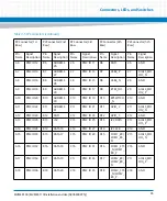
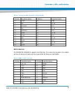
Page 61: ...J1 Front Panel Ethernet Connector J1 USB Connector J5 Table 3 1 Console Front Panel Connector J1 PIN No RS232 SIGNALING RS485 SIGNALING 1 NC NC 2 COM_0_RX COM_0_RX 3 COM_0_TX COM_0_TX 4 NC NC 5 GND GND 6 NC NC 7 COM_0_RTS COM0_TX 8 COM_0_CTS COM0_RX 9 NC NC Table 3 2 Front Panel Tri Speed Ethernet Connector J4 Note J4 is assembled only on ENP1 Pin No Signal Description 1 VCC 2 TD0 3 TD0 4 TD1 5 TD...

Page 62: ...ssembled only on ENP1 Pin No Signal Description Table 3 4 P1 Connectors P1 Connector 1st Row P1 Connector 2nd Row P1 Connector 3rd Row P1 Connector 4th Row P1 Connector 5th Row Pin Name Signal Description Pin Name Signal Description Pin Name Signal Description Pin Name Signal Description Pin Name Signal Description A1 DATA 0 B1 BBSY C1 DATA 8 D1 5V Z1 NC A2 DATA 1 B2 BCLR C2 DATA 9 D2 GND Z2 GND A...

Page 63: ...5 NC A16 DTACK B16 AM 0 C16 ADD 22 D16 3 3V not used Z16 GND A17 GND B17 AM 1 C17 ADD 21 D17 GA4 Z17 NC A18 AS B18 AM 2 C18 ADD 20 D18 3 3V not used Z18 GND A19 GND B19 AM 3 C19 ADD 19 D19 NC Z19 NC A20 IACK B20 GND C20 ADD 18 D20 3 3V not used Z20 GND A21 IACKIN B21 NC C21 ADD 17 D21 NC Z21 NC A22 IACKOUT B22 NC C22 ADD 16 D22 3 3V not used Z22 GND A23 AM 4 B23 GND C23 ADD 15 D23 NC Z23 NC A24 AD...

Page 64: ...d Row P2 Connector 4th Row P2 Connector 5th Row Pin Name Signal Description Pin Name Signal Description Pin Name Signal Description Pin Name Signal Description Pin Name Signal Description A1 PMC IO 2 B1 5V C1 PMC IO 1 D1 NC Z1 GIGE3_MD IO0_P A2 PMC IO 4 B2 GND C2 PMC IO 3 D2 NC Z2 GND A3 PMC IO 6 B3 RETRY C3 PMC IO 5 D3 GND Z3 GIGE3_MD IO0_N A4 PMC IO 8 B4 ADDRESS 24 C4 PMC IO 7 D4 USB1_P Z4 GND A...

Page 65: ...GND A13 PMC IO 26 B13 5V C13 PMC IO 25 D13 I2C DATA Z13 GIGE3_MD IO3_P A14 PMC IO 28 B14 DATA 16 C14 PMC IO 27 D14 I2C CLK Z14 GND A15 PMC IO 30 B15 DATA 17 C15 PMC IO 29 D15 COM1_RX COM1_RX_ N Z15 GIGE3_MD IO3_N A16 PMC IO 32 B16 DATA 18 C16 PMC IO 31 D16 COM1_CTS _N COM1_ RX_P Z16 GND A17 PMC IO 34 B17 DATA 19 C17 PMC IO 33 D17 COM2_RX COM2_RX_ N Z17 GIGE4_MD IO0_P A18 PMC IO 36 B18 DATA 20 C18 ...

Page 66: ...O1_N A24 PMC IO 48 B24 DATA 25 C24 PMC IO 47 D24 COM1_RTS _N COM1_ TX_P Z24 GND A25 PMC IO 50 B25 DATA 26 C25 PMC IO 49 D25 COM2_TX COM2_TX_ N Z25 GIGE4_MD IO2_P A26 PMC IO 52 B26 DATA 27 C26 PMC IO 51 D26 COM2_RTS _N COM2_ TX_P Z26 GND A27 PMC IO 54 B27 DATA 28 C27 PMC IO 53 D27 COM3_TX COM3_TX_ N Z27 GIGE4_MD IO2_N A28 PMC IO 56 B28 DATA 29 C28 PMC IO 55 D28 COM3_RTS _N COM3_ TX_P Z28 GND Table ...

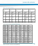
Page 67: ...P1_TX2_P GND P1_RX2_N P1_RX2_P 4 GND P1_TX3_N P1_TX3_P GND P1_RX3_N P1_RX3_P GND 5 NC GND SG_TX0_N SG_TX0_P GND SG_RX0_N SG_RX0_P 6 GND NC NC GND NC NC GND 7 GPIO0 GND NC NC GND NC NC 8 GND NC NC GND NC NC GND 9 GPIO1 GND NC NC GND NC NC 10 GND SATA_TX_N SATA_TX_P GND SATA_RX_N SATA_RX_P GND 11 NC GND SG_TX1_N SG_TX1_P GND SG_RX1_N SG_RX1_P 12 GND P2_TX0_N P2_TX0_P GND P2_RX0_N P2_RX0_P GND 13 NC ...

Page 68: ... connector SATA Connector The on board customized SATA connector is compatible with the Artesyn Embedded Technologies SATA kit MVME8100 HDMTKIT4 15 NC GND P2_TX3_N P2_TX3_P GND P2_RX3_N P2_RX3_P Table 3 6 VXS P0 Connector applicable to MVME8100 only continued Pin Row G Row F Row E Row D Row C Row B Row A Table 3 7 Customized SATA Connector J3 Pin Name Signal Description Pin Name Signal Description...

Page 69: ... 31 3 3V 12 SATA RX 32 5V 13 NC 33 3 3V 14 SATA RX 34 5V 15 GND 35 3 3V 16 GND 36 5V 17 NC 37 3 3V 18 GND 38 5V 19 NC 39 3 3V 20 GND 40 5V Table 3 8 PMC J11 J21 Connector Pin Name Signal Description Pin Name Signal Description 1 JTAG TCK 33 FRAME 2 12V 34 GND 3 GND 35 GND 4 INT A 36 IRDY 5 INT B 37 DEVSEL 6 INT C 38 5V 7 PRESENT SIGNAL 39 PCIXCAP 8 5V 40 LOCK 9 INT D 41 NC Table 3 7 Customized SAT...

Page 70: ...5V 19 3 3V 51 GND 20 AD 31 52 CBE0 21 AD 28 53 AD 6 22 AD 27 54 AD 5 23 AD 25 55 AD 4 24 GND 56 GND 25 GND 57 3 3V 26 CBE3 58 AD 3 27 AD 22 59 AD 2 28 AD 21 60 AD 1 29 AD 19 61 AD 0 30 5V 62 5V 31 3 3V 63 GND 32 AD 17 64 REQ64 Table 3 9 PMC J12 J22 Connector Pin Name Signal Description Pin Name Signal Description 1 12V 33 GND Table 3 8 PMC J11 J21 Connector continued Pin Name Signal Description Pi...

Page 71: ...0 NC 42 SERR 11 BUSMODE2 Pulled UP 43 CBE1 12 3 3V 44 GND 13 PCI RESET 45 AD 14 14 BUSMODE3 PULLED DWN 46 AD 13 15 3 3V 47 M66EN 16 BUSMODE4 PULLED DWN 48 AD 10 17 NC 49 AD 8 18 GND 50 3 3V 19 AD 30 51 AD 7 20 AD 29 52 REQB 21 GND 53 3 3V 22 AD 26 54 GNTB 23 AD 24 55 NC 24 3 3V 56 GND 25 IDSEL 57 NC 26 AD 23 58 EREADY Table 3 9 PMC J12 J22 Connector continued Pin Name Signal Description Pin Name S...

Page 72: ...gnal Description Pin Name Signal Description 1 NC 33 GND 2 GND 34 AD48 3 GND 35 AD 47 4 CBE7 36 AD 46 5 CBE6 37 AD 45 6 CBE5 38 GND 7 CBE4 39 3 3V 8 GND 40 AD 44 9 3 3V 41 AD 43 10 PAR64 42 AD 42 11 AD 63 43 AD 41 12 AD 62 44 GND 13 AD 61 45 GND 14 GND 46 AD 40 15 GND 47 AD 39 16 AD 60 48 AD 38 17 AD 59 49 AD 37 18 AD 58 50 GND Table 3 9 PMC J12 J22 Connector continued Pin Name Signal Description ...

Page 73: ... 50 62 GND 31 AD 49 63 GND 32 GND 64 NC Table 3 11 PMC J14 Connector Pin Name Signal Description Pin Name Signal Description 1 PMC IO 1 33 PMC IO 33 2 PMC IO 2 34 PMC IO 34 3 PMC IO 3 35 PMC IO 35 4 PMC IO 4 36 PMC IO 36 5 PMC IO 5 37 PMC IO 37 6 PMC IO 6 38 PMC IO 38 7 PMC IO 7 39 PMC IO 39 8 PMC IO 8 40 PMC IO 40 9 PMC IO 9 41 PMC IO 41 10 PMC IO 10 42 PMC IO 42 Table 3 10 PMC J13 J23 Connectors...

Page 74: ...IO 17 49 PMC IO 49 18 PMC IO 18 50 PMC IO 50 19 PMC IO 19 51 PMC IO 51 20 PMC IO 20 52 PMC IO 52 21 PMC IO 21 53 PMC IO 53 22 PMC IO 22 54 PMC IO 54 23 PMC IO 23 55 PMC IO 55 24 PMC IO 24 56 PMC IO 56 25 PMC IO 25 57 PMC IO 57 26 PMC IO 26 58 PMC IO 58 27 PMC IO 27 59 PMC IO 59 28 PMC IO 28 60 PMC IO 60 29 PMC IO 29 61 PMC IO 61 30 PMC IO 30 62 PMC IO 62 31 PMC IO 31 63 PMC IO 63 32 PMC IO 32 64 P...

Page 75: ...n 1 TCK 2 ASSET_PRSNT_L GNDon cable 3 TDO 4 GND 5 TMS 6 GND 7 TRST_L 8 GND 9 TDI 10 GND 11 No Pin Key 12 Reserved NC 13 GND 14 Reserved NC 15 GND 16 Reserved NC 17 GND 18 Reserved NC 19 GND 20 Reserved NC Table 3 13 XMC Connectors XJ1 2 ROW A XJ1 2 ROW B XJ1 2 ROW C XJ1 2 ROW D XJ1 2 ROW E XJ1 2 ROW F Pin No Signal Description Pin No Signal Description Pin No Signal Description Pin No Signal Descr...

Page 76: ...ENT 13 TX2 13 TX2 13 3 3V AUX 13 TX3 13 TX3 13 3 3V 14 GND 14 GND 14 GA 2 14 GND 14 GND 14 I2C DATA 15 TX4 15 TX4 15 NC 15 TX5 15 TX5 15 3 3V 16 GND 16 GND 16 MVMRO PULLED DOWN 16 GND 16 GND 16 I2C CLOCK 17 TX6 17 TX6 17 NC 17 TX7 17 TX7 17 NC 18 GND 18 GND 18 NC 18 GND 18 GND 18 NC 19 CLK 19 CLK 19 NC 19 NC 19 ROOT0 PULLED UP 19 NC Table 3 13 XMC Connectors continued XJ1 2 ROW A XJ1 2 ROW B XJ1 2...

Page 77: ...trollable Red User Software Controllable FAIL D8 Board Fail Off Normal operation after successful firmware boot Red One or more on board power rails have failed and the board has shutdown to protect the hardware Normal during power up during hardware reset such as a front panel reset May be asserted by the BDFAIL bit in the Tsi148 VSTAT register SPEED J4 Link Speed Off No link Amber 10 100BASE T o...

Page 78: ...w the board see Figure 3 1 on page 59 3 3 Switches The board provides the following configuration switches S2 Switch S3 Switch S4 Switch S5 Switch Reset Abort Switch Table 3 15 On board LEDs Status Label Function Color Description D32 MMC Write Protect off WP disabled Green WP enabled D33 ENP1 PS1_LED_N ENP4 Board FAIL Amber D34 ENP1 PS2_LED_N ENP4 POWER Green D35 ENP1 PS3_LED_N ENP4 RESET Amber D...

Page 79: ...ttings of switches marked as reserved The setting of switches which are not marked as reserved has to be checked and changed before board installation Table 3 16 S2 Switch Settings Position Default Description 1 OFF OFF Watchdog Disabled ON Watchdog Enabled 2 OFF OFF Serial Console Port to Front Panel ON Serial Console Port to P2 RTM panel 3 OFF OFF P2 Serial Port 0 is RS232 ON P2 Serial Port 0 is...

Page 80: ...s from P1 connector This switch reflects the inverted states on the geographical address signals 8 OFF OFF Select SRIO for P0 Backplane Fabric applicable to MVME8100 only ON Select PCIe for P0 Backplane Fabric applicable to MVME8100 only Table 3 16 S2 Switch Settings Position Default Description Table 3 17 S3 Switch Settings Position Default Description 1 OFF OFF SPI FLASH Write Protect is Disable...

Page 81: ... 11100 3 OFF OFF OFF ON OFF OFF 1 11011 4 ON OFF OFF ON OFF ON 0 11010 5 ON OFF OFF ON ON OFF 0 11001 6 OFF OFF OFF ON ON ON 1 11000 7 OFF OFF ON OFF OFF OFF 1 10111 8 ON OFF ON OFF OFF ON 0 10110 9 ON OFF ON OFF ON OFF 0 10101 10 OFF OFF ON OFF ON ON 1 10100 11 ON OFF ON ON OFF OFF 0 10011 12 OFF OFF ON ON OFF ON 1 10010 13 OFF OFF ON ON ON OFF 1 10001 14 ON OFF ON ON ON ON 0 10000 15 OFF ON OFF ...

Page 82: ...effective when the VME SCON AUTO switch is ON 3 3 1 4 S5 Switch The switch Bank S5 provides the boot SPI FLASH selection Table 3 19 S4 Switch Settings Position Default Description 1 OFF Clear Environment Variables OFF Disable Clear Environment Variables ON EnableClearEnvironmentVariables Atreset ubootENVvariablesare set to default values 2 OFF OFF Configure PCIe SRIo Switches as P0 Root Complex ap...

Page 83: ...tchcanfunctioneitherasaReset orAbortbutton Ifthebuttonispressedforlessthan3seconds theCPLDwillgenerateanabort interrupt to the P5020 P5010 processor If the button is pressed for more than 3 seconds the CPLD will generate a board hard reset If the board is configured as System Controller the backplane VME SYSRESET signal is also asserted during a board hard reset ...

Page 84: ...Connectors LEDs and Switches MVME8100 MVME8110 Installation and Use 6806800P25J 84 ...

Page 85: ... Functional Description The MVME8100 Single Board Computer is a 6U VME VXS board based on the Freescale QorIQ P5020 processor TheMVME8110SingleBoardComputerisa6UVMEboardbasedontheFreescaleQorIQP5010 processor This section describes the features of MVME8100 MVME8110 ...

Page 86: ...X DEMUX 2 PCIe Switch sRIO Switch PCIe x 1 PCIe to PCI X IDT TSI148 64 bit 133MHz PCI X VMEBus SATA SATA DDR3 ECC DDR3 ECC SATA CTRL SDHC SGMII SGMII SGMII PHY1 1000BASE T RGMII RGMII Dual PHY 1000BASE T 1000BASE T 1000BASE T SPI RJ45 MAG JACK USB USB USB Hub Quad UART RS XXX RS XXX RS XXX RS XXX Multi Protocol Transceiver 4 Multi Protocol Transceivers USB PORT Freescale QorIQ P5020 RS XXX Micro D...

Page 87: ...Functional Description MVME8100 MVME8110 Installation and Use 6806800P25J 87 Figure 4 2 illustrates the MVME8110 architecture Figure 4 2 Block Diagram of MVME8110 ...

Page 88: ...le also greatly simplifies the board design The MVME8100 board ENP1 version is designed to use the 2 0 GHz core processor version while the ENP4 version uses the 1 8 GHz processor The MVME8110 board ENP1 version is designed to use the 1 2 GHz core processor For more information refer P5020 P5010 QorIQ Integrated Multicore Communications Processor Family Reference Manual 4 3 System Memory The MVME8...

Page 89: ...process to turn on the RTC oscillator from Uboot MVME8100 i2c mm 0x68 e 1 0000000e 98 18 0000000f 80 n To set the date use the following uboot command MVME8100 date MMDDhhmm CC YY ss 4 4 2 P5020 P5010 Internal Timers The P5020 P5010 provides a total of eight global timers it is divided into two groups group A and group B Each group has four timers Each timer has four individual configuration regis...

Page 90: ...Command Status Register 4 4 3 2 OS Watchdog The OS Watchdog OSWD is not armed after reset It is enabled right after the IWD is disabled The OSWD timeout is set to 108s If the timer terminates the OSWD reset sequence will be initiated OSWD is serviced and disabled by writing 0xBBC2 to CPLD Command Status Register 4 4 4 CPLD Tick Timer The MVME8100 supports four independent 32 bit timers that are im...

Page 91: ...and dTSEC2 in SGMII mode for two additional 1000Base BX Ethernet ports to P0 4 6 SPI Interface Firmware boot Flash resides on the P5020 P5010 eSPI bus interface 4 6 1 SPI Flash Memory The P5020 P5010 contains two Eight MB serial flash devices These devices contain the 512 bits of the Reset Configuration Word the boot firmware image U boot and the ENV environment variables 4 6 2 Firmware Redundancy...

Page 92: ...RX TX RTS and CTS signals Only four wire full duplex RX TX is supported in RS422 485 mode The signaling mode is selected through on board configuration switches The default baud rate on the front panel serial is 9600 baud The physical front panel console connector is a male micro min DB 9 A male to male micro mini DB9 to DB9 adapter cable is available under Artesyn Embedded Technologies Part Numbe...

Page 93: ...of the switch is configured to operate at Gen 1 data rate The configuration of the ports and the partitioning of the switch into a single or multiple domains is controlled by an I2C eeprom connected to the PCIe switch master SMbus and loaded into the switch following reset The board provides two separate eeproms so that separate configuration data can be maintained for the MVME8100 MVME8110 operat...

Page 94: ...rate This port is routed to an IDT 80HCPS1616 SRIO switch for expansion of the SRIO ports The SRIO switch supports multiple lane speeds including 1 25 2 5 3 125 and 5 0 Gbaud The MVME8100 provides two x4 SRIO ports which may be routed to the P0 connector through a high speed mux The selection of SRIO or PCIe ports to P0 is controlled by the S2 8 configuration switch see S2 Switch on page 79 The co...

Page 95: ...end point eeprom for loading the configuration data after reset is determined by the root complex configuration switch S4 2 see S4 Switch on page 82 The eeproms can be reprogrammed over the processor I2C bus 4 interface The eeprom device addresses are listed in section I2C Devices on page 98 A diagram of the SRIO port topology is shown in the figure below The 80HCPS1616 SRIO switch does not suppor...

Page 96: ... and Environmental Layer for PCI Mezzanine Card VITA 42 for XMC VITA 42 3 PCIe for XMC PMC XMC sites are keyed for 3 3V PMC signaling MVME8100 MVME8110 provides a x8 PCI Express interface link for PMC XMC1 and x4 PCI Express interface link for PMC XMC2 It is designed such that same PCI Express interface is used foreithertheXMCorthePCIetoPCI XbridgerequiredforaPMC Thisismadepossiblebyusing Pericom ...

Page 97: ...gned to support an optional 2 5 inch SATA HDD SDD in PMC XMC site 2 The heat frame has mounting holes to support the 2 5 SSD HDD on board The connector interface to the MVME8100 MVME8110 board is compatible with the Artesyn Embedded Technologies SATA mounting kit MVME8100 HDMTKIT4 which contains a SATA adapter board screws and mounting brackets The SATA adapter board provides a standard SATA conne...

Page 98: ...rovides two USB 2 0 controllers with integrated PHYs The MVME8100 MVME8110 routes USB port 1 to the front panel to an upright USB Type A receptacle The DC power for the front panel USB port is supplied through Micrel s MIC2076 power switch which provides soft current limiting over current detection and power enable The P5020 P5010 USB port 2 is routed to a USB2512 hub device which provides two add...

Page 99: ...terfacepinsthrough the JTAG connector It uses a 1 8 MHz oscillator for logic control The CPLD provides the following functions Power control and fault detection Reset sequence and reset management Figure 4 5 I2C Busses CPU FREESCALE U79 I2C_1 I2C_4 PCIE EP EEPROM U20 SRIO SWITCH U104 RTM VPD EEPROM 0x51 local 0x54 0x52 0x6E 0x6E 0x5D 0x74 0x57 SRIO RC EEPROM U6 0x55 PCIE SW1 RC EEPROM U3 0x68 RTC ...

Page 100: ...ment The 5 volt coming from the back plane is utilized to derive all on board voltage rails To provide therequiredvoltagesequencing eachvoltagerailiscontrolledbytheCPLDthroughenablepin of each regulator and the output is being monitored by CPLD through each regulator power good signal If one voltage rail fails the CPLD will disable all of the regulators and the only way to restart the board is by ...

Page 101: ...20RGYT 1 3 A max 1 2V_SW TPS54620RGYT 1 2 1 5A max 2 5V LTC3026EDD PBF 1 5 A max IDT32NT24AG2 IDT CPS 1616 Marvell88SE9125 Freescale P5020 P5010 Freescale P5020 P5010 DDR3 Memory Devices IDT TSI148 Pericom PI 3L301 DAE Pericom PI 2PCIE2412 Marvell 88SE9125 IDT TSI 384 Broadcom BCM54616S Broadcom BCM5482SHA2IFBG IDT CPS 1616 Freescale P5020 P5010 Broadcom BCM 54616 S Broadcom BCM5482SHA2 IFBG IDT32...

Page 102: ... 133Mhz LVCMOS 133Mhz LVCMOS 25Mhz LVCMOS TSI 148 TSI 384 VME P5020 P5010 SYSCLK P5020 P5010 ETH CTRL 1 2 88SE9125 SATA CTRL 32NT24AG2 GCLK0 32NT24AG2 GCLK1 88SE9125 SATA CTRL 1 8432MHz OSC CPLD 1 8432MHz QUART 1 8432MHz 32 768 KHz P5020 P5010 RTC 80HCPS1616 SRIO SW 24MHz OSC USB2512 HUB 24Mhz P5020 P5010 USB 100 Mhz Differential HCSL 100 Mhz Differential HCSL P5020 P5010 SERDES REF1 P5020 P5010 S...

Page 103: ...P25J 103 4 21 Reset Structure The MVME8100 MVME8110 reset begins after the power up sequence is completed A board reset can also be initiated using the front panel reset switch the RTM reset switch through P2 or under software control through the processor Reset Request ...

Page 104: ...R_V1P0_IDT_PWRGD PWR_V1P2_SW_PWRGD PWR_V1P5_ PWRGD PWR_VTT_ PWRGD PWR_V3P3_ MISC_ EN FRONT PANEL SW FPSWITCH _N CPU_ HRESET _N CPU_ PORESET _N CPU_ RESET_REQ_ N 5V_ PGOOD TSI384 88SE 9125SATA 32NT24 PCIe SW TSI384 TSI384 PCIE_ PERST_BR1_N PCIE_ PERST_BR2_N PCIE_ PERST_BR3_N PCIE_PERST_SATA_N _ PCIESW 1_PERST_N TSI148 PCI X VME Bridge VSYSRESETO To VME Bus PURST_N LSRSTI _N TSI148_PLL_RSTI_N LRSTO ...

Page 105: ...2 from LED_P2 2 pin IRQ3 GPIO21 QUART_IRQ0 Quart Interrupt INTA IRQ4 GPIO22 QUART_IRQ1 Quart Interrupt INTB IRQ5 GPIO23 QUART_IRQ2 Quart Interrupt INTC IRQ6 GPIO24 QUART_IRQ3 Quart Interrupt INTD IRQ7 GPIO25 CPLD_TEMP_INT_L Board Temperature interrupt routed through CPLD IRQ8 GPIO26 CPLD_TIMER_INT_L CPLD Internal Timers and Abort IRQ IRQ9 GPIO27 BCM54616S INT BCM54616S PHY interrupt from LED4 pin ...

Page 106: ...curacy on the remote sensor and 3C accuracy on the internal sensor The ADT7461 registers can be used to configure the low temperature limit and high temperature limit for the local sensor as well as for the remote sensor Aninterruptcanbegeneratediflimitsareexceeded TheTMP112Atemperaturesensor isusedtomeasurethetemperatureattheboardedgeoppositefromtheCPU Sincetheairflow direction can be different i...

Page 107: ... and Use 6806800P25J 107 However to maintain proper CPU temperature the recommended air flow direction is to enter the board from the CPU side that is the air should flow in the direction from PMC XMC site 1 to PMC XMC Site 2 Figure 4 9 Thermal Management ...

Page 108: ...Functional Description MVME8100 MVME8110 Installation and Use 6806800P25J 108 ...

Page 109: ... procedures that are specific to the MVME8100 MVME8110 For general information on U Boot see http www denx de wiki U Boot WebHome 5 1 Accessing U Boot 1 Connecttheboardtoacomputerwithaserialinterfaceconnectorandaterminalemulation software running on it The serial connector of the board is found on the face plate 2 Configure the terminal software to use the access parameters that are specified in U...

Page 110: ...he TFTP server 2 Configure U Boot environment variables setenv ipaddr IP address of MVME8100 MVME8110 setenv serverip IP address of TFTP server setenv gatewayip gateway IP setenv netmask netmask setenv bootargs root dev ram rw console ttyS0 9600n8 ramdisk_size 700000 cache sram size 0x10000 saveenv 3 Transfer the files through the TFTP from the server to the local memory tftp 1000000 kernel_image ...

Page 111: ...2load scsi 0 1 2000000 File_ramdisk ext2load scsi 0 1 f00000 File_dtb 4 Boot the Linux in memory bootm 1000000 2000000 f00000 5 2 3 Booting from a USB Drive 1 Make sure that the kernel dtb and ramdisk are saved in the USB drive with FAT partition 2 Configure the U Boot environment variable setenv File_uImage kernel_image setenv File_dtb kernel dtb setenv File_ramdisk ramdisk saveenv 3 Initialize U...

Page 112: ... File_dtb 5 Boot the Linux in memory bootm 1000000 2000000 f00000 5 2 5 Booting VxWorks Through the Network In this mode the U Boot downloads and boots VxWorks from an external TFTP server 1 Make sure that the VxWorks image is accessible by the board from the TFTP server 2 Configure U Boot environment variables setenv ipaddr IP address of MVME8100 MVME8110 setenv serverip IP address of TFTP server...

Page 113: ... run bootcmd bootelf Boot from an ELF image in memory bootm Boot application image from memory bootp Boot image through network using BOOTP TFTP protocol bootvx Boot VxWorks from an ELF image cmp Memory compare coninfo Print console devices and information cp Memory copy cpu Multiprocessor CPU boot manipulation and release crc32 Checksum calculation date Get set reset date time diags Runs POST dia...

Page 114: ... serial line kermit mode loads Load S Record file over serial line loady Load binary file over serial line ymodem mode loop Infinite loop on address range md Memory display memmap Displays memory map mii MII utility commands mm Memory modify auto incrementing address mmc MMC sub system mmcinfo Display MMC info moninit Reset nvram serial and write monitor to SPI flash mtest Simple RAM read write te...

Page 115: ...ent storage script Run a delimited terminated list of commands scsi SCSI sub system scsiboot Boot from SCSI device setenv Set environment variables setexpr Set environment variable as the result of eval expression sf SPI flash sub system showvar Print local hushshell variables sleep Delay execution for some time soft_reset Soft reset the board source Run script from memory test Minimal test like b...

Page 116: ...e Mount Technology SMT Configuration Switch S3 1 is in the OFF position 2 Select SPI flash 0 sf probe 0 3 Erase 0x90000 bytes starting at SPI address 0 sf erase 0 0x90000 4 Write 0x90000 bytes from RAM address 0x1000000 starting at SPI address 0 sf write 0x1000000 0 0x90000 To replace the image in SPI bank 1 replace step 2 with Select SPI flash 1 sf probe 1 ...

Page 117: ...MVME8110 Installation and Use 6806800P25J 117 A Battery Exchange A 1 Battery Exchange The ENP1 variant contains an on board battery The battery location is shown in the following figure Figure A 1 Battery Location Battery ...

Page 118: ...ardous explosion When exchanging the on board lithium battery make sure that the new and the old battery are exactly the same battery models If the respective battery model is not available contact your local Artesyn Embedded Technologies sales representative for the availability of alternative officially approved battery models Data Loss Exchanging the battery can result in loss of time settings ...

Page 119: ...you are looking for 3 In the Search text box type the product name and click GO B 2 Related Specifications For additional information refer to the following table for related specifications As an additional help a source for the listed document is provided Please note that while these sources have been verified the information is subject to change without notice Table B 1 Artesyn Embedded Technolo...

Page 120: ...I Local Bus Specification Revision 2 2 PCI Rev 2 2 December 18 1998 PCI XElectricalandMechanicalAddendumtothePCILocalBusSpecification Revision 2 0a PCI X EM 2 0a August 22 2003 PCI X Protocol Addendum to the PCI Local Bus Specification Revision 2 0a PCI X PT 2 0a July 22 2003 Institute for Electrical and Electronics Engineers Inc IEEE Standard for a Common Mezzanine Card CMC Family IEEE1386 Oct 25...

Page 121: ...s provided Please note that while these sources have been verified the information is subject to change without notice Table B 3 Manufacturer s Publications Document Title and Source Publication Number Freescale Corporation P5020 P5010 QorIQ Integrated Processor Hardware Specifications P5020EC P5020 QorIQ Integrated Multicore Communication Processor Reference Manual P5020RM Integrated Devices IDT ...

Page 122: ...Related Documentation MVME8100 MVME8110 Installation and Use 6806800P25J 122 ...

Page 123: ......

Page 124: ...esyn and the Artesyn Embedded Technologies logo are trademarks and service marks of Artesyn Embedded Technologies Inc All other product or service names are the property of their respective owners 2015 Artesyn Embedded Technologies Inc ...

Reviews: