background image

Maps and Registers

ATCA-7360 Installation and Use (6806800J07S

)

166

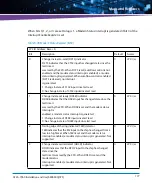
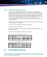
6.3.4.2

UART Registers DLAB=0

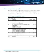
6.3.4.2.1 Receiver Buffer Register (RBR)

In non-FIFO mode, this register holds the character received by the UART's Receive Shift 
Register. If fewer than eight bits are received, the bits are right-justified and the leading bits are 
zeroed. Reading the register, empties the register and resets the Data Ready (DR) bit in the Line 
Status Register to zero. Other (error) bits in the Line Status Register are not cleared. In FIFO 
mode, this register latches the value of the data byte at the top of the FIFO.

6.3.4.2.2 Transmitter Holding Register (THR)

This register holds the next data byte to be transmitted. When the Transmit Shift Register 
becomes empty, the contents of the Transmit Holding Register are loaded into the shift 
register and the transmit data request (TDRQ) bit in the Line Status Register is set to one.

In FIFO mode, writing to THR puts data to the top of the FIFO. The data at the bottom of the 
FIFO is loaded to the shift register when it is empty.

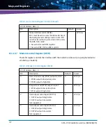
Table 6-27 Receiver Buffer Register (RBR) if DLAB=0 

LPC IO Address: Base

Bit

Description

Default

Access

7:0

Receiver Buffer Register (RBR)

Undefined

LPC: r

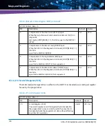
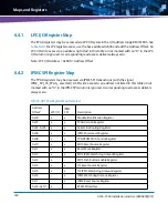
Table 6-28 Transmitter Holding Register (THR) if DLAB=0 

LPC IO Address: Base

Bit

Description

Default

Access

7:0

Transmitter Holding Register (THR)

Undefined

LPC: w

Summary of Contents for ATCA-7360

Page 1: ...ATCA 7360 Installation and Use P N 6806800J07S May 2016...

Page 2: ...an Artesyn website The text itself may not be published commercially in print or electronic form edited translated or otherwise altered without the permission of Artesyn It is possible that this publ...

Page 3: ...he Blade 45 2 2 Environmental and Power Requirements 46 2 2 1 Environmental Requirements 46 2 2 2 Power Requirements 50 2 3 Blade Layout 52 2 4 Switch Settings 53 2 5 Installing Blade Accessories 55 2...

Page 4: ...3 Changing Configuration Settings 89 4 4 Boot Options 91 4 4 1 Supported Boot Devices 91 4 4 2 Selecting The Boot Device 91 4 4 3 By Boot Selection Menu 93 4 4 4 iSCSI Setup for Base and Fabric Ether...

Page 5: ...ve Exit 114 4 6 CPU Performance Settings 115 4 7 Memory Configuration 115 4 7 1 Independent Channel Mode 116 4 7 2 Spare Channel Mode 116 4 7 3 Mirrored Channel Mode 116 4 7 4 Lockstep Channel Mode 11...

Page 6: ...sistent memory 143 5 4 Chipset 143 5 5 I O Controller 143 5 6 Firmware Flashes 144 5 7 Ethernet Ports 145 5 8 Storage Controller 145 5 9 Embedded Flash Disk 145 5 9 1 SATA Embedded Flash Solid State D...

Page 7: ...edirection Control Register 182 6 4 6 Serial Over LAN SOL Control Register 183 6 4 7 Serial Line Routing Register 184 6 4 8 IPMC Power Level Register 184 6 4 9 SPD PROM MUX Control Register 185 6 4 10...

Page 8: ...ck Supervision Registers 207 6 4 22 1 Telecom Clocking Status Registers 207 6 4 22 2 Telecom Timer Registers 208 6 4 23 Miscellaneous Status Control Registers 209 6 4 24 Scratch Registers 210 7 Serial...

Page 9: ...Set Hardware Address Command 246 8 4 8 Get Handle Switch Command 247 8 4 9 Set Handle Switch Command 248 8 4 10 Get Payload Communication Time Out Command 248 8 4 11 Set Payload Communication Time Ou...

Page 10: ...l 275 10 1 2 1 Update Procedure 275 10 1 3 Interface 276 10 1 3 1 KCS Interface 276 10 1 3 2 IPMB 0 276 10 1 3 3 LAN over Ethernet BASE 277 10 2 IPMC Upgrade 277 10 3 BIOS FPGA Upgrade 278 10 4 Upgrad...

Page 11: ...el R VT for Directed I O Configuration 103 Table 4 9 Chipset North Bridge IOH Thermal Sensors 103 Table 4 10 Chipset South Bridge 104 Table 4 11 Chipset South Bridge USB Configuration 104 Table 4 12 A...

Page 12: ...ble 4 42 Correctable Memory Log Disabled Event Format 130 Table 4 43 Memory Information Definition 130 Table 4 44 Log Area Reset Cleared Event Format 130 Table 4 45 System Boot Event Format 131 Table...

Page 13: ...mon Decode Ranges 163 Table 6 22 Logical Device Primary Interrupt Register 163 Table 6 23 Logical Device 0x74 Reserved Register 164 Table 6 24 Logical Device 0x75 Reserved Register 164 Table 6 25 Logi...

Page 14: ...Interrupt Status Register 194 Table 6 60 Processor Hot Status Control Register 195 Table 6 61 Telecom Status Control Register 196 Table 6 62 Address Map of Interrupt Mask and Map Registers 196 Table 6...

Page 15: ...8 9 System Boot Options Parameter 96 222 Table 8 10 System Boot Options Parameter 97 223 Table 8 11 System Boot Options Parameter 98 224 Table 8 12 System Boot Options Parameter 100 Data Format 226 T...

Page 16: ...Command 252 Table 8 42 Get Payload Shutdown Time Out Command 253 Table 8 43 Set Payload Shutdown Time Out Command 254 Table 8 44 Get Module State Command 254 Table 8 45 Enable Module Site Command 256...

Page 17: ...le Connector 78 Figure 3 14 USB Flash Module Connector Pin Assignment 79 Figure 3 15 Location of AdvancedTCA Connectors 80 Figure 3 16 P10 Backplane Connector Pinout 81 Figure 3 17 P20 Backplane Conne...

Page 18: ...ping on ATCA 7360 154 Figure 7 1 SOL Overview 211 Figure 8 1 System Boot Options Parameter 100 Information Flow Overview 225 Figure 9 1 Location of Temperature Sensors 267 Figure 10 1 IPMC Component E...

Page 19: ...on and removal procedures Controls Indicators and Connectors on page 67 describes external interfaces of the blade This includes connectors and LEDs BIOS on page 87 describes the features and setup of...

Page 20: ...emiconductor DDR Double Data Rate DIMM Dual Inline Memory Module DMA Direct Memory Access DPLL Digital Phase Locked Loop DRAM Dynamic Random Access Memory ECC Error Correction Code EMC Electromagnetic...

Page 21: ...L Red Hat Enterprise Linux RTC Real Time Clock RTM Rear Transition Module RoHS Restriction of the use of Certain Hazardous Substances SAS Serial Attached SCSI SATA Serial ATA SCSI Small Computer Syste...

Page 22: ...n screenoutputandcoderelatedelements or commands in body text Courier Bold Used to characterize user input and to separate it from system output Reference Used for references and for table and figure...

Page 23: ...us situation which if not avoided could result in death or serious injury Indicates a hazardous situation which if not avoided may result in minor or moderate injury Indicates a property damage messag...

Page 24: ...ble Get Handle Switch Command on page 247 and Table Set Handle Switch Command on page 248 Updated Table Environmental Requirements on page 47 6806800J07K April 2012 Updated Table 2 3 and a note in DIM...

Page 25: ...on page 264 Added Figure A 1 on page 281 Moved location of Safety Notes on page 27 and Sicherheitshinweise on page 31 Changed faceplate labels OK to IS and ATN to ATTN Added Figure P10 Backplane Conne...

Page 26: ...ATCA 7360 Installation and Use 6806800J07S About this Manual 26 About this Manual...

Page 27: ...ation industry and industrial control Only personnel trained by Artesyn or persons qualified in electronics or electrical engineering are authorized to install remove or maintain the product The infor...

Page 28: ...ance with this guide may cause harmful interference to radio communications Operating the system in a residential area is likely to cause harmful interference in which case the user will be required t...

Page 29: ...Blade surface High humidity and condensation on the blade surface causes short circuits Do not operate the blade outside the specified environmental limits Make sure the blade is completely dry and t...

Page 30: ...nd changed before blade installation Blade Damage Setting resetting the switches during operation can cause blade damage Therefore check and change switch settings before you install the blade Battery...

Page 31: ...den Sie sich bitte an die f r Sie zust ndige Gesch ftsstelle von Artesyn Das System erf llt die f r die Industrie geforderten Sicherheitsvorschriften und darf ausschlie lich f r Anwendungen in der Tel...

Page 32: ...Kabel So stellen Sie sicher dass ausreichend Schutz vor St rstrahlung vorhanden ist Die Blades m ssen mit der Frontblende installiert und alle freien Steckpl tze m ssen mit Blindblenden abgedeckt sei...

Page 33: ...ugabe von prim ren Schutz nicht ausreichenden Schutz um diese Schnittstellen metallisch mit OSP Verdrahtung verbinden Die intra Geb ude Port s des Ger tes oder einer Unterbaugruppe m ssen abgeschirmte...

Page 34: ...ind k nnen mit produktionsrelevanten Funktionen belegt sein Das ndern dieser Schalter kann im normalen Betrieb St rungen ausl sen Verstellen Sie nur solche Schalter die nicht mit Reserved gekennzeichn...

Page 35: ...se ATCA 7360 Installation and Use 6806800J07S 35 Umweltschutz Entsorgen Sie alte Batterien und oder Blades Systemkomponenten RTMs stets gem der in Ihrem Land g ltigen Gesetzgebung und den Empfehlungen...

Page 36: ...ATCA 7360 Installation and Use 6806800J07S Sicherheitshinweise 36...

Page 37: ...each CPU 10 sockets in total Max 80 GB 10 x 8 GB Intel 5520 I O hub spanning 36 PCIe Gen2 lanes 5 Gbps 4 GB onboard USB flash module assembly option with capacity up to 16GB PCIe Generation 2 with 5...

Page 38: ...EN 300019 series 1 The blade does not fulfill the Unpacked Equipment Shock Criteria as defined in NEBS GR63 4 3 2 During tests whichconsistedofdroppingthebladefrom100mmheight weobservedthatonsomeblad...

Page 39: ...nted inside the shelf for example at the backplane or the shelf has to provide a possibility to lead Logic Ground out of the shelf for external connection to Central Office Ground For further informat...

Page 40: ...X 2GB 10G support ATCA 7360 24GB ATCA processor blade dual L5518 quad core 2 13 GHz 6X 4GB 10G support ATCA 7360 48GB ATCA processor blade dual L5518 quad core 2 13 GHz 6X 8GB 10G support Table 1 4 Bl...

Page 41: ...SATA for ATCA 736X product series2 ATCA7360 SFMMOD Reset persistent memory 16MB SRAM 64MB Flash for the ATCA 736X product series2 RJ45 DSUB ATCA7140 RJ 45 DSUB cable for the ATCA 7140 7150 7350 736X...

Page 42: ...Introduction ATCA 7360 Installation and Use 6806800J07S 42 1 5 Product Identification The following figure illustrates the location of the serial number label Figure 1 1 Serial Number Location...

Page 43: ...Introduction ATCA 7360 Installation and Use 6806800J07S 43...

Page 44: ...Introduction ATCA 7360 Installation and Use 6806800J07S 44...

Page 45: ...d report any damage or differences to the customer service 3 Remove the desiccant bag shipped together with the blade and dispose of it according to your country s legislation Damage of Circuits Elect...

Page 46: ...at least the CP TA B 4 cooling profile The environmental requirements of the blade may be further limited down due to installed accessories such as hard disks or mezzanine modules with more restrictiv...

Page 47: ...hange 0 25 C min according to Telcordia GR 63 CORE 0 25 C min Rel Humidity Normal Operation 5 rH to 85 rh non condensing Exceptional Operation 5 rH to 90 rh non condensing According to Telcordia GR 63...

Page 48: ...g are not exceeded If not stated otherwise the temperatures should be measured by placing a sensor exactly at the given locations Table 2 2 Critical Temperature Limits Component Thermal Design Power M...

Page 49: ...0 Q51 MHS4 P23 CE31 Q77 Q50 R3627 R3628 R3629 R3630 R3635 R3636 R3651 R3652 F10 F7 F8 F11 MHS3 R1597 R1598 R1615 Q55 Q51 C3692 C3686 R3616 R3615 L83 C4053 MHS4 R2719 C4715 Q78 Q77 C3710 C3704 C3698 C3...

Page 50: ...mentation delivered together with the respective accessory or consult your local Artesyn representative for further details The blade must be connected to a TNV 2 or a safety extra low voltage SELV ci...

Page 51: ...simultaneously exercising as many functions and interfaces as possible This includes a particular load software provided by Intel designed to stress the processors to reach their theoretical maximum p...

Page 52: ...Installation ATCA 7360 Installation and Use 6806800J07S 52 2 3 Blade Layout The following figure illustrates the location of components on the ATCA 7360 Figure 2 2 ATCA 7360 Blade Layout...

Page 53: ...witches marked as Reserved The setting of switches which are not marked as Reserved has to be checked and changed before blade installation Blade Damage Setting resetting the switches during operation...

Page 54: ...sh security descriptor and ME disabled for debugging only SW2 1 Serial Line 1 and 2 Routing OFF FPGA COM 1 to faceplate FPGA COM 2 to RTM default ON FPGA COM 1 to RTM FPGA COM 2 to faceplate SW2 2 IPM...

Page 55: ...Timer system reboot feature OFF ICH10 TCO Timer system reboot feature enabled default ON ICH10 will disable the TCO Timer system reboot feature SW4 1 ICH10 TOP Swap override OFF Default ON system is...

Page 56: ...Forthermalreasons no4 rank DIMMs and no dual Die DIMM are allowed Installation Procedure To install a DIMM module proceed as follows 1 Remove the blade from system as described in Installing and Remov...

Page 57: ...er memory modules 2 5 2 PMEM and SATA Module The PMEM SATA extension slot allows assembly of either a PMEM or SATA module which are available as upgrade kits for ATCA 7360 PMEM module consists of an S...

Page 58: ...ATA module proceed as follows 1 Remove the blade from the system as described in Installing and Removing the Blade on page 60 2 Plug the PMEM SATA module on the blade so that the module s standoffs fi...

Page 59: ...blade 4 Reinstall the blade into the system as described in Installing and Removing the Blade on page 60 2 5 3 USB 2 0 Flash Module ThebladesprovidesaUSB2 0flashmodulewithacapacityof4GBor16GB Thecorr...

Page 60: ...e To install a USB flash module proceed as follows 1 Remove blade from system as described in Removing the Blade on page 64 2 Insert new flash module into the socket see figure Figure 2 2 on page 52 3...

Page 61: ...d as follows Damage of Circuits Electrostatic discharge and incorrect blade installation and removal can damage circuits or shorten their life Before touching the blade or electronic components make s...

Page 62: ...ottom ejector handles are in the outward position by squeezing the lever and the latch together 2 Insert blade into the shelf by placing the top and bottom edges of the blade in the card guides of the...

Page 63: ...to blink This indicates that the blade has signified its presence its presence to the shelf management controller 6 Wait until the blue LED is switched off then fasten the faceplate screws which secu...

Page 64: ...otate the handle fully outward The blue LED blinks indicating that the blade power down process is ongoing 2 Wait until the blue LED is illuminated permanently then unlatch the upper handle and rotate...

Page 65: ...if applicable 4 Unfasten the screws of the faceplate until the blade is detached from the shelf 5 Remove the blade from the shelf Data Loss Removing the blade with the blue LED still blinking causes d...

Page 66: ...Installation ATCA 7360 Installation and Use 6806800J07S 66...

Page 67: ...3534 D54 R1247 C1481 R1219 C4340 C1463 C1453 R1235 R1236 R1238 R1243 R1223 J220 T220 C3026 J117 L20 R2753 R2755 R2770 R2772 R2777 R2779 C4668 C4669 C4670 C4672 C4675 C4678 C4683 C4686 R1240 R2809 R281...

Page 68: ...ntrols Indicators and Connectors ATCA 7360 Installation and Use 6806800J07S 68 3 2 Faceplate The following figure illustrates the connectors keys and LEDs available at the faceplate Figure 3 2 Facepla...

Page 69: ...ontrols Indicators and Connectors ATCA 7360 Installation and Use 6806800J07S 69 3 2 1 LEDs The following figure illustrates all the LEDs available at the faceplate Figure 3 3 Location of Faceplate LED...

Page 70: ...green red amber and is programmable via IPMC Its default color is green and its local control state is off It permits override control by higher layer software such as middle ware or applications as...

Page 71: ...tallation Permanently blue On board IPMC powers up Blinking blue Blade communicates with shelf manager OFF Blade is active During blade removal Blinking blue Blade notifies shelf manager of its desire...

Page 72: ...One Serial Two USB 3 2 3 1 Ethernet Connector The blade provides one Ethernet 1000Base T interface connector at its faceplate It is intended for blade configuration and constitutes besides the two Ad...

Page 73: ...ch 2 1 allows to swap COM1 with COM2 and thus make COM2 accessible via the faceplate connector instead Note that the BIOS serial redirection feature uses COM1 as access interface Therefore swapping th...

Page 74: ...ade provides two USB connectors at its faceplate They are compliant to the USB 2 0 standard and correspond to the blade s USB interfaces 3 and 4 Their location is shown in the following figure Figure...

Page 75: ...The PMEM SFMEM Module connects to the blade through a connector that carries the following types of signals PCI interface signals I2C signals for connection with on board IDROM device Four configurati...

Page 76: ...s Indicators and Connectors ATCA 7360 Installation and Use 6806800J07S 76 The location of the PMEM SFMEM module connector is shown in the following figure Figure 3 11 Location of PMEM SFMEM Module Con...

Page 77: ...Controls Indicators and Connectors ATCA 7360 Installation and Use 6806800J07S 77 The pinout of this connector is shown in the following figure Figure 3 12 PMEM SATA Module Connector Pinout...

Page 78: ...Connectors ATCA 7360 Installation and Use 6806800J07S 78 3 3 2 USB Flash Module Connector The location of the flash memory module connector is shown in the following figure Figure 3 13 Location of USB...

Page 79: ...CA 7360 Installation and Use 6806800J07S 79 You can find the pin assignment of the flash connector in the following figure Figure 3 14 USB Flash Module Connector Pin Assignment 1 3 5 7 9 2 4 6 8 10 US...

Page 80: ...edTCA Backplane Connectors The AdvancedTCA backplane connectors reside in the three zones 1 to 3 as specified by the AdvancedTCA standard and are called P10 P20 and 23 and P30 and 32 The pinouts of al...

Page 81: ...r feed for the blade VM48_x_CON and RTN_x_CON Power enable ENABLE_x IPMB bus signals IPMB0_x_yyy Geographic address signals HAx Ground signals SHELF_GND and GND Reserved signals Zone 2 contains the tw...

Page 82: ...al in the AdvancedTCA specification and are unused on the blade If the AdvancedTCA specification defines these signals as input signals they are terminated on the blade and marked as TERM_ in the foll...

Page 83: ...Controls Indicators and Connectors ATCA 7360 Installation and Use 6806800J07S 83 Figure 3 18 P20 Backplane Connector Pinout Rows E to H Figure 3 19 P23 Backplane Connector Pinout Rows A to D...

Page 84: ...ns the two connectors P30 and P32 They are used to connect an RTM to the blade and carry the following signals Serial RS232_x_yyyy Serial ATA SATAx_yyy USB USBxy PCI Express PCIEx_yyy IPMI IPMB1_xxx I...

Page 85: ...7360 Installation and Use 6806800J07S 85 SAS Update channels General control signals BD_PRESENTx RTM_PRSNT_N RTM_RST_KEY RTM_RST Figure 3 21 P30 Backplane Connector Pinout Rows A to D Figure 3 22 P30...

Page 86: ...Controls Indicators and Connectors ATCA 7360 Installation and Use 6806800J07S 86 Figure 3 23 P32 Backplane Connector Pinout Rows A to D Figure 3 24 P32 Backplane Connector Pinout Rows E to H...

Page 87: ...blade is based on the AMI UEFI BIOS with several Artesyn extensions integrated Its main features are Initialize CPU chipset and memory Initialize PCI devices Setup utility for setting configuration da...

Page 88: ...as a normal PC keyboard input The serial console redirection feature can be configured via a setup utility 4 2 1 Requirements for Serial Console Redirection For serial console redirection the followin...

Page 89: ...minal The following communication parameters are used by default Baud rate 9600 Flow control None VT 100 8 data bits No parity 1 stop bit 4 2 3 Connecting to the Blade Procedure To connect to the blad...

Page 90: ...bottom of the menu Additionally an item specific help is displayed on the right side of the menu window Figure 4 1 Main Menu Make sure that BIOS is properly configured prior to installing the operati...

Page 91: ...SATA interface available only when SSD SATA is assembled Storage devices connected to the SAS controller by RTM Network Front Panel Ethernet Base Ethernet and Ethernet on RTM Storage devices connected...

Page 92: ...r of the devices from which BIOS attempts to boot the operating system 3 Enter the submenu Option Rom Execution to enable disable booting from specific devices Changes have to be saved and the board h...

Page 93: ...1 From the menu select Save Exit 2 Override existing boot sequence by selecting another boot device from the boot override list Figure 4 2 Save and Exit Menu If the selected device does not load the o...

Page 94: ...rom the menu select Boot 2 Under the Option ROM Execution sub menu select the iSCSI item of Fabric Network Boot setup option 3 Save and Exit the BIOS setup 4 To enter iSCSI setup press Ctrl D when fol...

Page 95: ...the iSCSI Port Selection screen The following table provides information about Ethernet Port Mapping Figure 4 4 iSCSI Port Selection Table 4 2 Ethernet port mapping Network Device iSCSI Option ROM De...

Page 96: ...Configure iSCSI port Discard Save and Exit menu items Table 4 3 Select iSCSI Boot priority hot keys Key Function P Selected device is primary boot device S Selected device is secondary boot device D D...

Page 97: ...ation and Use 6806800J07S 97 4 4 4 3 iSCSI Boot Configuration The following figure depicts the iSCSI Boot Configuration screen Enter Initiator and Target network configuration parameter Figure 4 6 iSC...

Page 98: ...4 4 4 4 iSCSI Challenge Handshake Authentication Protocol CHAP Configuration The following figure depicts the iSCSI CHAP Configuration screen Enter Challenge Handshake Authentication Protocol configur...

Page 99: ...Configuration Item Values Description Hyper threading Enabled Default Disabled Enabled for OS optimized for Hyper Threading Technology Disabled for other OS not optimized for Hyper Threading Technolo...

Page 100: ...Turbo Mode Enabled Default Disabled Enable Disable Turbo Mode Turbo Mode allows processor cores to run faster than the marked frequency if the physical processor is operating below power temperature...

Page 101: ...ation See Memory Configuration on page 115 NUMA Enable Default Disable Enable Disable support for Non uniform Memory Access NUMA aware Operating Systems Select Enable for NUMA aware OS e g Windows Ser...

Page 102: ...s detected during normal read write operation the correct data and ECC check bits will be written back to memory Table 4 6 Memory Configuration continued Item Values Description Table 4 7 Chipset Nort...

Page 103: ...ne Interrupt Remapping support Coherency Support Enable Disable Default Enable Disable VT d Engine Coherency support ATS Support Enable Disable Default Enable Disable VT d Engine Address Translation S...

Page 104: ...Enable Default Disable Enable Disable the High Precision Event Timer Table 4 11 Chipset South Bridge USB Configuration Item Values Description All USB Devices Enabled Default Disabled Enable Disable...

Page 105: ...ompatible work in IDE compatible mode Only available when SATA Mode is set to IDE mode SATA Controller 1 Disable Enhanced Default Disable or select mode of Serial ATA Controller 1 Enhanced work in SAT...

Page 106: ...according to their media format Devices less than 530MB are detected as floppies Optical drives are emulated as CD ROM drives with no media will be emulated according to a drive type Forced FDD option...

Page 107: ...T100 VT UTF8 Default ANSI VT UTF8 is the preferred terminal type for out of band Windows EMS management The next best choice is VT100 and then VT100 Table 4 16 Serial Port Console Redirection Console...

Page 108: ...equire more than 1 stop bit Recorder Mode Enabled Disabled Default On this mode enabled only text will be send This is to capture Terminal data Resolution 100x31 Enabled Disabled Default Enables or di...

Page 109: ...able all features of SMBIOS Event Logging during boot Erase Event Log No Default Yes On next reset Yes On every reset Choose options for erasing SMBIOS Event Log Erasing is done prior to any logging a...

Page 110: ...does not take effect until the computer is restarted Table 4 21 Advanced WHEA Configuration Item Values Description WHEA Support Enable Disable Default Enable or disable support for Windows Hardware...

Page 111: ...s to shut off the watchdog timer when successfully booted O S Watchdog Timer Timeout 1 2 3 5 7 10 15 20 minutes Default 5 minutes Configure the time out of the O S Boot Watchdog Timer Not available if...

Page 112: ...Mask for the Initiator Network Not available when DHCP is enabled GateWay Enter IP Address of Gateway Not available when DHCP is enabled Get target info via DHCP Enable Disable Default Get target inf...

Page 113: ...el Net Boot Enabled Default Disabled ControlsexecutionoftheOptionROMfortheFrontPanel Ethernet controller Select Enabled when Front Panel Boot is required Base Network Boot Enabled Default Disabled Con...

Page 114: ...nnel Boot is required Table 4 26 Boot Option ROM Execution continued Item Values Description Table 4 27 Save Exit Item Values Description Save Changes and Exit Exit BIOS setup after saving the changes...

Page 115: ...ine Prefetch Enabled L1 Data Prefetcher Enabled DataReuse Optimization Enabled Enterprise Platforms Hardware Prefetcher Disabled Adjacent Cache Line Prefetch Disabled L1 Data Prefetcher Disabled DataR...

Page 116: ...This means that all three channels must have identical population with regards to size and organization DIMM slot populations The Memory Controller will maintain correctable ECC error counters for ea...

Page 117: ...ion of these cases Detection of all permutations of 2 x4 DRAM failures 4 8 Restoring BIOS Default Settings The blade provides an on board configuration switch that allows to load BIOS settings from th...

Page 118: ...t up progress In boot loader phase PEI phase U1 and U2 glow red U3 is glowing alternately red green and orange In main initialization phase DXE phase only U3 is glowing alternately red green and orang...

Page 119: ...MBIOS error logging IPMI event logging Error logging to the console 4 12 1 Runtime Error Logging BIOS supports Runtime Error Logging for memory errors and PCI errors See BIOS Setup Advanced Runtime Er...

Page 120: ...ror Simulation For test purposes it is possible to inject errors Enable Inject Errors in Event Logs SMBIOS Event Log Settings in BIOS setup The following errors are injected short before the OS is boo...

Page 121: ...BIOS ATCA 7360 Installation and Use 6806800J07S 121 These errors are logged to SMBIOS error log IPMI error log local SEL and Shelf manager and to the console...

Page 122: ...IST Error 22h PCI Out Of Resource 50h IPMI Boot Parameter Default Area Read Error 51h IPMI Boot Parameter Default Area Locked 52h IPMI Boot Parameter Default Area Checksum Error 53h IPMI Boot Paramete...

Page 123: ...fset 00h No bootable media no boot device found Battery 29h Offset 01h Battery failed System Firmware Progress 0Fh Offset 00h System Firmware Error 70h Front Panel Network not detected 78h Base Networ...

Page 124: ...ent log area can be obtained from the DMI structure System Event Log Type 15 The DMI table can be read by the Linux tool dmidecode The Log Change Token in SMBIOS Type 15 structure is not supported The...

Page 125: ...emory Error event format Offset Name Format Description 00h Event Type BYTE Event Type 01h 01h Length BYTE always 0Ch 02h 07h Date Time Fields BYTE These fields contain the BCD representation of the d...

Page 126: ...s contain the BCD representation of the date and time 08h 0Bh Memory Information UINT32 OEM extension Table 4 33 Memory Information Definition Bit Description 0 7 reserved 8 15 DIMM number per Channel...

Page 127: ...OEM IPMI failure 29 OEM IPMI Boot Parameter read write error 30 OEM IPMI Boot Parameter checksum error 31 OEM IPMI Boot Parameter locked Table 4 36 Result Second DWORD supported POST Errors Bit Descri...

Page 128: ...ion Table 4 37 PCI Parity Error Event Format Offset Name Format Description 00h Event Type BYTE Event Type 09h 01h Length BYTE always 0Ch 02h 07h Date Time Fields BYTE These fields contain the BCD rep...

Page 129: ...00h Event Type BYTE Event Type 0Ah 01h Length BYTE always 0Ch 02h 07h Date Time Fields BYTE These fields contain the BCD representation of the date and time 08h 0Bh PCI Information UINT32 OEM extensi...

Page 130: ...og Disabled Event Format Offset Name Format Description 00h Event Type BYTE Event Type 01h 01h Length BYTE always 0Ch 02h 07h Date Time Fields BYTE These fields contain the BCD representation of the d...

Page 131: ...mat Offset Name Format Description 00h Event Type BYTE Event Type 17h 01h Length BYTE always 08h 02h 07h Date Time Fields BYTE These fields contain the BCD representation of the date and time Table 4...

Page 132: ...framework download htm 4 12 4 10 1Artesyn OEM Extensions Class Computing Unit Table 4 47 Status Code Type Definition Bit Description 0 7 Type 2 Error Code 8 23 reserved 24 31 Severity 4 Minor 8 Major...

Page 133: ...as booted a OS the reading of the POST code sensor returns no valid status code 800Dh North Bridge Error Table 4 51 SubClass EFI_COMPUTING_UNIT_FIRMWARE_PROCESSOR 02h IPMI Operation Code Description 8...

Page 134: ...0 0xCF DXE execution up to BDS 0xD0 0xDF DXE errors 0xE0 0xE8 S3 Resume PEI 0xE9 0xEF S3 Resume errors PEI 0xE8 0xEF Memory initialization errors 0xB0 0xBF Additional Memory Initialization Status Code...

Page 135: ...loaded Table 4 54 PEI Status Codes Status Code Description Progress Codes 0x10 PEI Core is started 0x15 Pre memory North Bridge initialization is started 0x19 Pre memory South Bridge initialization i...

Page 136: ...y memory controller initialization 0xB6 Check DIMM population 0xB7 Channel initialization 0xB8 Channel training 0xB9 Run Build In Self Test 0xBA Initialize memory map 0xBB Setup RAS configuration 0xBF...

Page 137: ...0xF3 Recovery firmware image is found 0xF4 Recovery firmware image is loaded 0xF5 0xF7 Reserved for future AMI progress codes Recovery Error Codes 0xF8 Recovery PPI is not available 0xF9 Recovery cap...

Page 138: ...lize Boot Variables 0x90 Boot Device Selection BDS phase is started 0x91 Driver connecting is started 0x92 PCI Bus initialization is started 0x93 PCI Bus Hot Plug Controller Initialization 0x94 PCI Bu...

Page 139: ...Legacy Option ROM Initialization 0xB3 System Reset 0xB4 USB hot plug 0xB5 PCI bus hot plug 0xB6 Clean up of NVRAM 0xB7 Configuration Reset reset of NVRAM settings DXE Error Codes 0xD0 CPU initializati...

Page 140: ...8 Invalid password 0xD9 Error loading Boot Option LoadImage returned error 0xDA Boot Option is failed StartImage returned error 0xDB Flash update is failed 0xDC Reset protocol is not available Table 4...

Page 141: ...Ie x4 PCIe x4 PCIe x4 PCIe x4 Zone 3 X F M R 10 100 1000Base T ICH10 PHY 82567 PMEM SATA Module SATA 4GB SSD ESI PCI SATA SATA USB2 0 ICH10 Port 0 2 USB2 0 ICH10 Port 6 SPI Debug Socket Rec SPI SPI FP...

Page 142: ...nsions 3 SSE3 and Streaming SIMD Extensions 4 SSE4 The processor supports several Advanced Technologies Execute Disable Bit Intel 64 Technology Enhanced Intel SpeedStep Technology Intel Virtualization...

Page 143: ...timesfour PCIe lanes routed to the Zone 3 connector The chipset is connected to the ICH10R I O Controller via the Enterprise South Bridge Interface ESI 5 5 I O Controller The ICH10R provides extensive...

Page 144: ...Primary or Default BIOS Flash SPI 0 Recovery BIOS Flash SPI 1 The flash is allocated for storing the binary code of the BIOS The ATCA 7360 boots from the primary flash SPI 0 under normal circumstances...

Page 145: ...disk drive located on the RTM is connected to the controller A minimum of two 2 ports are available on the RTM faceplate They can be used to attach an external storage RAID JBOD Another SAS port of t...

Page 146: ...ons to access the payload hardware The IPMC firmware FW is stored in two independent memory images Crisis recovery control is provided to allow reboot of the IPMC from a 2nd image if the upgraded FW i...

Page 147: ...put from the standard keyboard The console typically is used by the BIOS setup menus BIOS initialization and boot routines OS boot loaders and loaded OS The serial console of the payload CPU is availa...

Page 148: ...e SOL based serial console 5 14 Control Logic The blade provides control logic for specific functions including Payload power supervision and sequencing Payload resets Multiple HW interfaces between p...

Page 149: ...DDR3 DIMM memory modules I2 C Bus Repeater of type PCA9515 is used to buffer the SMBus portion going to the SPD PROMs on the DIMM The BIOS reads memory configuration parameters from SPD PROM To addres...

Page 150: ...nsumes 0 9 uA hr Theoptionalpower downbackupmethodusesaSuperCAPwitha1Faradcapacity This provides 300 hours of RTC SRAM backup The default battery is an external 3 V lithium battery with a capacity of...

Page 151: ...CH10R supports 16 interrupts 8 external signal inputs The IO APIC device inside the ICH10R supports 24 interrupt sources In APIC mode the ICH10R supports only front side bus interrupt delivery not the...

Page 152: ...ic IRQ7 via SERIRQ PIRQ Slave 8 Internal RTC Internal RTC Timer 1 HPET 9 Generic IRQ9 via SERIRQ SCI TCO or PIRQ 10 Generic IRQ10 via SERIRQ SCI TCO or PIRQ 11 Generic IRQ11 via SERIRQ SCI TCO or PIRQ...

Page 153: ...ISA legacy style interrupts via SERIRQ 3 4 5 6 7 8 RTC Timer 1 legacy mode 9 Option for TCI TCO 10 Option for TCI TCO 11 Timer 2 Option for TCI TCO 12 Timer 3 13 FERR logic 14 SATA Primary legacy mod...

Page 154: ...6 2 on page 154 6 3 Registers For register description the convention shown in Table 6 4 Register Default and Table 6 5 Register Access Type are used Table 6 3 PCIexpress Port mapping Port 1 2 3 4 5 6...

Page 155: ...ter Access Type Access Description r Read only w Write only r w Read and write w1c Write 1 to clear ignore bit while reading r w1c Read and write 1 to clear write 0 has no effect r w1s Read and write...

Page 156: ...ecoded by the LPC core 6 3 1 1 2 LPC Memory Decoding The LPC interface never responds to LPC Memory accesses 6 3 1 1 3 LPC Firmware Decoding The LPC interface never responds to LPC Firmware accesses T...

Page 157: ...The two nibbles of the register are converted to 7 segment codes and are displayed as two hex values by two 7 segment LED Displays The IPMC may read the POST code using the SPI interface with the sign...

Page 158: ...en the Super IO is in the Configuration State When the Super IO is not in the Configuration State reads return 0xFF and write data is ignored 6 3 3 1 Entering the Configuration State The device enters...

Page 159: ...1 Global Control Configuration Registers The Super IO Global Registers lie in the address range 0x00 0x2F All eight bits of the ADDRESS port are used for register selection All unimplemented registers...

Page 160: ...gical device This allows access to the control and configuration registers for each logical device 0 LPC r w Table 6 13 Super IO Device Identification Register Index Address 0x20 Bit Description Defau...

Page 161: ...r These registers are then accessed through the DATA PORT The logical device registers are accessible only when the device is in the configuration state Table 6 16 Global Super IO SERIRQ and Pre divid...

Page 162: ...Access 0 Logical Device Enable 0 disabled Currently selected device is inactive 1 enabled The currently selected device is enabled 1 LPC r w 7 1 Reserved 0 LPC r Table 6 19 Logical Device Base IO Add...

Page 163: ...0x2F8 0x2FF COM2 0x2E8 0x2EF COM3 0x3E8 0x3EF COM4 Table 6 22 Logical Device Primary Interrupt Register Index Address 0x70 Bit Description Default Access 3 0 Interrupt level is used for Primary Inter...

Page 164: ...gister to a non zero value and setting any combination of bits 0 4 in the corresponding UART IER and the occurrence of the corresponding UART event that is Modem Status Change Receiver Line Error Cond...

Page 165: ...UART Register Overview LPC IO Address DLAB Bit value Description Base 0 Receiver Buffer RBR Read Only Base 0 Transmitter Holding THR Write Only Base 1 0 Interrupt Enable Register IER Base 2 X Interru...

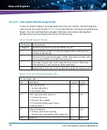
Page 166: ...of the FIFO 6 3 4 2 2 Transmitter Holding Register THR This register holds the next data byte to be transmitted When the Transmit Shift Register becomes empty the contents of the Transmit Holding Reg...

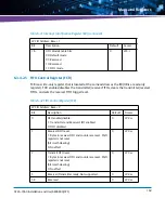
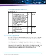
Page 167: ...le 6 29 Interrupt Enable Register IER if DLAB 0 LPC IO Address Base 1 Bit Description Default Access 0 Receive data interrupt enable disable 1 receive data interrupt enabled 0 receive data interrupt d...

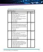
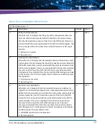
Page 168: ...level was reached in non FIFO mode RBR has data 2 Receiver Time out occurred It happens in FIFO mode only when there is data in the receive FIFO but no activity for a time period 3 Transmitter reques...

Page 169: ...6 31 Interrupt Identification Register IIR continued LPC IO Address Base 1 Bit Description Default Access Table 6 32 FIFO Control Register FCR LPC IO Address Base 2 Bit Description Default Access 0 FI...

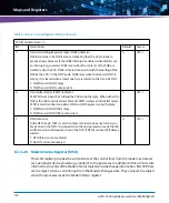
Page 170: ...ontents of the Line Control Register The read capability simplifies system programming and eliminates the need for separate storage in system memory 7 6 Receiver FIFO interrupt trigger level 00 1 byte...

Page 171: ...f logic ones is selected 1 Even parity 0 Odd parity 0 LPC r w 5 Stick parity When bits 3 4 and 5 are set the parity bit is transmitted and checked as cleared When bits 3 and 5 are set and bit 4 is cle...

Page 172: ...R and IER registers 0 LPC r w Table 6 33 Line Control Register LCR continued LPC IO Address Base 3 Bit Description Default Access Table 6 34 Modem Control Register MCR LPC IO Address Base 4 Bit Descri...

Page 173: ...FIFO has errors the LSR error bits are set and are not cleared until software reads LSR even if the character in the FIFO is read and a new character is now at the top of the FIFO 4 Local loop back d...

Page 174: ...ion Default Access 0 Receiver data ready DR indicator DR is set whenever a complete incoming character has been received and transferred into the RBR or the FIFO DR is cleared by reading all of the da...

Page 175: ...nize after a framing error To accomplish this it is assumed that the framing error is due to the next start bit The ACE samples this start bit twice and then accepts the input data 1 Framing error occ...

Page 176: ...he TSR THRE is cleared concurrent with the loading of the THR by the CPU In the FIFO mode THRE is set when the transmit FIFO is empty it is cleared when at least one byte is written to the transmit FI...

Page 177: ...ut since last read 0 LPC r w 1 Change in data set ready DDSR indicator DDSR indicates that the DSR input has changed state since the last time it was read by the CPU When DDSR is set and the modem sta...

Page 178: ...mplement of the ring indicator RI input When the ACE is in the diagnostic test mode LOOP MCR4 1 this bit is equal to the MCR bit 2 OUT1 Not supported Ext LPC r 7 Complement of the data carrier detect...

Page 179: ...nter is immediately loaded This prevents long counts oninitial load Access to the Divisor latch can be done with a word write The UART_CLK is the CLK_UART 48MHz input divided by the pre divider set by...

Page 180: ...MC_SPI_SS_FPGA_ asserted A SPI write access to an address not listed in this table or not marked with an X in the IPMC SPI column is ignored A corresponding read access delivers always zero Table 6 40...

Page 181: ...5 x x SFMEM Module Configuration Register 0x48 x x Update Channel Equalization Control 0x49 x IPMC E Keying Status Register 0x4A x x IPMC E Keying Control Register 0x4B x IPMC GPIO Register 0x50 x x L...

Page 182: ...ease 6 4 5 Serial Redirection Control Register BIOS set the corresponding bit which is used for serial redirection The IPMC uses this information to route the corresponding port to serial IPMC interfa...

Page 183: ...al redirection 1 COM1 used for serial redirection 0 LPC r w IPMC r 1 COM2 use for serial redirection 0 COM2 not used for serial redirection 1 COM2 used for serial redirection 0 LPC r w IPMC r 7 2 Rese...

Page 184: ...may be overwritten by IPMC Software 00 COM1 to faceplate and COM2 to RTM 01 COM1 to RTM and COM2 to faceplate 10 Reserved 11 Reserved Ext SW2 21 SW2 1 00 OFF OFF 01 OFF ON 10 ON OFF 11 ON ON 1 The Si...

Page 185: ...X0_IN LPC r IPMC r w 5 SMBUS_MUX1_OUT 2 0 SMBUS_MUX1_OUT is driven low 1 SMBUS_MUX1_OUT is driven high 2 When the SPD PROM MUX is locked by BIOS Bit 7 is set the signal level of SMBUS_MUX1_IN is read...

Page 186: ...ive at the same time OS should never write to this register Table 6 48 BIOS Reset Source Register Address Offset 0x10 Bit Description Default Access 0 PWR_GOOD Payload Power on reset 1 Reset occurred...

Page 187: ...testhattheassociatedresetisenabled Azeroindicates that the associated reset source is masked 7 IPMC_RST_ REQ_ Payload Reset from IPMC 1 Reset occurred PWR_GOOD 0 LPC r w1c IPMC r Table 6 48 BIOS Reset...

Page 188: ...ister The BIOS needs to write to this register to enable the Front Panel push button reset the RTM push button reset and the IPMC reset OS should never write to this register Table 6 50 BIOS IPMC Watc...

Page 189: ...wo reset sources go active at the same time Table 6 51 BIOS Push Button Enable Register Address Offset 0x13 Bit Description Default Access 7 0 BIOS Push Button Enable Register LPC w BIOS should never...

Page 190: ...Debugger reset 1 Reset occurred PWR_GOOD 0 LPC r w1c IPMC r 7 IPMC_RST_ REQ_ Payload Reset from IPMC 1 Reset occurred PWR_GOOD 0 LPC r w1c IPMC r Table 6 52 Reset Source Register continued Address Of...

Page 191: ...MC Watchdog Timeout Register and Table 6 53 OS IPMC Watchdog Timeout Register are set IPMC needs to clear the IPMC watchdog timeout bit to arm IPMC watchdog timeout event recognition Table 6 54 IPMC W...

Page 192: ...same time Table 6 55 IPMC Reset Source Register Address Offset 0x17 Bit Description Default Access 0 PWR_GOOD Payload Power on reset 1 Reset occurred PWR_GOOD 1 IPMC r w1c 1 XDP0_BRD_PWROK CPU Debugge...

Page 193: ...rminates when SPI transaction has finished A write access to the RTM SPI Address Command Register with the Command Bit 0 Write starts a SPI write transaction The value of the RTM SPI Write Register is...

Page 194: ...M Interrupt Status Register The RTM Interrupt Status Register will be located in the RTM SPI address space The host can access the RTM register using the RTM SPI Master Interface No RTM interrupt sour...

Page 195: ...Master face is active the current level is latched Ext LPC r 1 When an interrupt is active the corresponding status bit is read 1 Table 6 59 External Interrupt Status Register continued Address Offset...

Page 196: ...has an Interrupt Mask and Map Register See the table below Table 6 61 Telecom Status Control Register Address Offset 0x22 Bit Signal Description Default Access 0 CH1_CLK1A_IN Clock CLK1A of Chassis 1...

Page 197: ...from IOH Thermo sensor 0x28 APB_ALARM A 48V input alarm low voltage etc 0x29 RTM_SPI_MISO RTM interrupt sources 0x2A CPU0_PRCHT_ CPU0 Processor hot interrupt 0x2B CPU1_PRCHT_ CPU1 Processor hot interr...

Page 198: ...e number 1 IRQ0 0x02 Frame number 2 IRQ1 0x03 Frame number 3 IRQ2 SMI_ 0x04 Frame number 4 IRQ3 0x05 Frame number 5 IRQ4 0x06 Frame number 6 IRQ5 0x07 Frame number 7 IRQ6 0x08 Frame number 8 IRQ7 0x09...

Page 199: ...ap Interrupt to CPU_IRQ_F_ 0x6 Map Interrupt to CPU_IRQ_G_ 0x7 Map Interrupt to CPU_IRQ_H_ 0 LPC r w Table 6 63 Interrupt Mask and Map Registers continued Address Offset 0x23 0x2D Bit Description Defa...

Page 200: ...3 1 OFF 1 SW3 1 ON LPC r 6 Manual Boot Flash select Signal BOOT_DEFAULT Used when SW3 1 is ON 0 Selects Default Boot SPI Flash 1 Selects Recover Boot SPI Flash Ext 0 SW3 2 OFF 1 SW3 2 ON LPC r 7 IPMC...

Page 201: ...isable A write value 0xC3 enables the Flash All other values disables the Flash LPC w Table 6 67 BIOS Boot Mode Register Address Offset 0x43 Bit Description Default Access 0 1 The switch signals SW_BI...

Page 202: ...RX 0 UC1_EQ_RX is driven low 1 UC1_EQ_RX is tri state 0 LPC r w IPMC r 1 Control output Signal UC1_EQ_TX 0 UC1_EQ_TX is driven low 1 UC1_EQ_TX is tri state 0 LPC r w IPMC r 2 Control output Signal UC2...

Page 203: ...nal UC4_EQ_TX 0 UC4_EQ_TX is driven low 1 UC4_EQ_TX is tri state 0 LPC r w IPMC r Table 6 69 Update Channel Equalization Control Register continued Address Offset 0x48 Bit Description Default Access T...

Page 204: ...S_ driven low Disabled 1 BASEIF_LAN0_DIS_ driven high Enabled 1 LPC r w IPMC r w 3 Enable Disable Base IF 2 0 BASEIF_LAN1_DIS_ driven low Disabled 1 BASEIF_LAN1_DIS_ driven high Enabled 1 LPC r w IPMC...

Page 205: ...ister Address Offset 0x50 Bit Description Default Access 0 Control green LED output Signal LED_GREEN_ 0 LED_GREEN_ is driven high 1 LED_GREEN_ is driven low 0 LPC r w IPMC r 1 Control read LED output...

Page 206: ...SEL controlled by IPMC Ext r Table 6 73 LED Status and Control Register continued Address Offset 0x50 Bit Description Default Access Table 6 74 NMI Status and Control Register Address Offset 0x58 Bit...

Page 207: ...n the clock is static or the period is higher than a 16 bit value the result is always 0xFFFF Table 6 75 Telecom Backplane Clocking Status Register Address Offset 0x66 Bit Description Default Access 0...

Page 208: ...programmed from 1 to 65535 which allows timeout values from 125 sec to 8 191875sec based on an 8kHz input clock When a timeout occurs the timer is 0 the timeout bit is set See Table 6 61 Telecom Stat...

Page 209: ...Telecom Timer MSB Register Address Offset 0x65 Bit Description Default Access 7 0 MSB of Telecom Timer start value PWR_GOOD 0 LPC r w Table 6 82 Telecom Timer LSB Register Address Offset 0x64 Bit Des...

Page 210: ...atch Registers Table 6 84 LPC Scratch Register Address Offset 0x45 Bit Description Default Access 7 0 LPC Scratch bits PWR_GOOD 0 LPC r w IPMC r Table 6 85 IPMC Scratch Register Address Offset 0x45 Bi...

Page 211: ...SOL session SOL is only available on the base interface The sideband interface of the Intel 82576 in pass through mode is used to transmit receive its terminal characters via the base interface You ca...

Page 212: ...onfigure SOL Parameters You can configure the following SOL parameters You can use standard IPMI commands or the ipmitool to modify the parameters 7 3 1 Using Standard IPMI Commands This example shows...

Page 213: ...Commit ipmicmd k f 0 c 1 5 0 2 smi 0 7 3 2 Using ipmitool The example below shows how to setup a LAN configuration parameter for a potential SOL session with ipmitool for Base Ethernet Channel 1 chann...

Page 214: ...teway IP 172 16 0 1 Default Gateway MAC 00 00 00 00 00 00 RMCP Cipher Suites 1 2 3 3 Cipher Suite Priv Max Not Available root localhost ipmitool lan print 6 Set in Progress Set Complete Auth Type Supp...

Page 215: ...detailed above are fulfilled 2 Compile and install the ipmitool on your target which is destined for opening the SOL session on the ATCA 7360 for details refer to Installing the ipmitool on page 211 3...

Page 216: ...7360 SOL interface ipmitool C 1 I lanplus H 172 16 0 221 U soluser P solpasswd k gkey sol activate For details on the command parameters refer to the ipmitool documentation available on http ipmitool...

Page 217: ...lades providing a system interface Table 8 1 Supported Global IPMI Commands Command NetFn Request Response CMD Comments Get Device ID 0x06 0x07 0x01 Cold Reset 0x06 0x07 0x02 Warm Reset 0x06 0x07 0x03...

Page 218: ...0x07 0x42 Set User Access 0x06 0x07 0x43 Get User Access 0x06 0x07 0x44 Set User Name 0x06 0x07 0x45 Get User Name 0x06 0x07 0x46 Set User Password 0x06 0x07 0x47 Set User Payload Access 0x06 0x07 0x...

Page 219: ...Response CMD Get SEL Info 0x0A 0x0B 0x40 Reserve SEL 0x0A 0x0B 0x42 Get SEL Entry 0x0A 0x0B 0x43 Add SEL Entry 0x0A 0x0B 0x44 Clear SEL 0x0A 0x0B 0x47 Get SEL Time 0x0A 0x0B 0x48 Set SEL Time 0x0A 0x...

Page 220: ...0x05 0x24 Get Sensor Hysteresis 0x04 0x05 0x25 Set Sensor Threshold 0x04 0x05 0x26 Most of the threshold based sensors have fixed thresholds Before using this command check whether threshold setting...

Page 221: ...different purposes When using the Get Set System Boot Options commands except for parameter 100 use the response request data fields with the Set Selector and the Block Selector set to 0x00 When usin...

Page 222: ...A configuration stream load 0 Load configuration stream from default boot flash 1 Load configuration stream from backup boot flash Note The new FPGA configuration stream is loaded into the FPGA at the...

Page 223: ...ystem Boot Options Parameter 97 Data Byte Description 1 POST Type Data 1 Set Selector This is the processor ID for which the boot option is to be set 2 Data 2 POST Type Selector This parameter is used...

Page 224: ...Note that the boot parameters in the IPMC storage area have higher priority than the same boot options which may be configured in the firmware itself for example via the setup menu The storage area is...

Page 225: ...in the default area Details are given in the following sections The following figure summarizes the previously explained basic information flow related to the system boot options parameter 100 On some...

Page 226: ...m Boot Options Parameter 100 Data Format Byte Description 0 1 Number of bytes used for boot parameters LSB first The number of bytes must be calculated and written into these two bytes by the software...

Page 227: ...to write to Index 0 refers to the first block of 16 bytes which includes the first two bytes which indicate the boot parameter data size Depending on the total length of the boot option data your sof...

Page 228: ...ge not supported by the IPMC 0xC9 block selector is outside of the allowed range 2 Reserved Set to 1 3 Bit 7 If set to 1 the addressed storage area is locked Bits 6 0 value 100 indicating this OEM boo...

Page 229: ...gs made in the BIOS setup menu and the settings specified via the System Boot Options command 100 Changing a parameter in either of these automatically changes the respective value in the other Table...

Page 230: ...rd SATA device 5 Onboard SATA sashdd SAS HDD mounted on the RTM sas0_nn SAS Controller nn SCSI ID use this when a SAS array is connected to the RTM frontnet Front Panel Network basenet0 Base Ethernet...

Page 231: ...l Up to 8 boot devices are supported Example boot_order sas0_03 basenet0 usbkey sata1 Table 8 16 boot_order Devices continued Device Description Table 8 17 Supported LAN Device Commands Command NetFn...

Page 232: ...blade supports the cold reset and graceful reboot options Get FRU LED Properties 0x2C 0x2D 0x05 Get FRU LED Color Capabilities 0x2C 0x2D 0x06 Set FRU LED State 0x2C 0x2D 0x07 Get FRU LED State 0x2C 0x...

Page 233: ...apabilities 0x2C 0x2D 0x2E Get component properties 0x2C 0x2D 0x2F Abort firmware upgrade 0x2C 0x2D 0x30 Initiate upgrade action 0x2C 0x2D 0x31 Upload firmware block 0x2C 0x2D 0x32 Finish firmware upl...

Page 234: ...ng any of these commands the shelf management software must check whether the receiving IPMI controller supports Artesyn specific IPMI commands by using the IPMI command Get Device ID Sending Artesyn...

Page 235: ...rprise number A value of 0x65 has to be used 3 MSB of Artesyn IANA Enterprise number A value of 0x00 has to be used 4 Serial connector type 0 Faceplate connector 1 Backplane connector All other values...

Page 236: ...y only BIOS output is supported Table 8 22 Request Data of Get Serial Output Command Byte Data Field 1 LSB of Artesyn IANA Enterprise number A value of 0xCD has to be used 2 Second byte of Artesyn IAN...

Page 237: ...0x00 Get Serial Interface Properties Table 8 27 on page 241 0x2E 0x2F 0x01 Set Serial Interface Properties Table 8 28 on page 242 0x2E 0x2F 0x02 Get Debug Level Table 8 29 on page 243 0x2E 0x2F 0x03...

Page 238: ...e 8 25 IPMC Modes Mode Description Standalone In standalone mode the carrier IPMC disconnects from IPMB 0 but keeps on listening to the serial debug and payload interfaces and serving requests coming...

Page 239: ...aceful Reboot Request Ifsetto1 indicatesthatthepayloadisrequestedtoinitiatethe graceful reboot sequence Bit 6 Diagnostic Interrupt Request If set to 1 indicates that a payload diagnostic interrupt req...

Page 240: ...rrived from the shelf manager 0 Metallic Bus 1 Query 1 Metallic Bus 1 Release 2 Metallic Bus 1 Force 3 Metallic Bus 1 Free 7 Bits 4 7 Clock Bus 2 Events These bits indicate pending Clock Bus 2 request...

Page 241: ...lf manager 0 Clock Bus 3 Query 1 Clock Bus 3 Release 2 Clock Bus 3 Force 3 Clock Bus 3 Free Table 8 26 Get Status Command continued Type Byte Data Field Table 8 27 Get Serial Interface Properties Comm...

Page 242: ...ce Bits 6 4 Reserved Bits 3 0 Baud Rate ID The baud rate ID defines the interface baud rate as follows 0 9600 bps 1 19200 bps 2 38400 bps 3 57600 bps unsupported 4 115200 bps unsupported Table 8 27 Ge...

Page 243: ...00 bps unsupported 4 115200 bps unsupported Response Data 1 Completion Code 2 4 PPS IANA Private Enterprise ID 0x00400A 16394 Pigeon Point Systems LSB Byte first byte 2 0A byte 3 40 byte 4 00 Table 8...

Page 244: ...ovides a trace of IPMB messages that are arriving to going from the IPMC via IPMB O Bit 3 n a Bit 2 Alert Logging Enable Ifsetto1 theIPMCoutputsimportantalertmessagesonto the serial debug interface Bi...

Page 245: ...ing to going from the IPMC via IPMB O Bit 3 n a Bit 2 Alert Logging Enable If set to 1 the IPMC outputs important alert messages onto the serial debug interface Bit 1 Low level Error Logging Enable If...

Page 246: ...a 1 3 PPS IANA Private Enterprise ID 0x00400A 16394 Pigeon Point Systems LSB Byte first byte 1 0A byte 2 40 byte 3 00 Response Data 1 Completion Code 2 4 PPS IANA Private Enterprise ID 0x00400A 16394...

Page 247: ...first byte 2 0A byte 3 40 byte 4 00 Table 8 32 Set Hardware Address Command continued Type Byte Data Field Table 8 33 Get Handle Switch Command Type Byte Data Field Request Data 1 3 PPS IANA Private...

Page 248: ...3 PPS IANA Private Enterprise ID 0x00400A 16394 Pigeon Point Systems LSB Byte first byte 1 0A byte 2 40 byte 3 00 4 FRU ID specify as 0 5 Handle Switch Status 0x00 The handle switch is open 0x01 The...

Page 249: ...ion time out may vary from 0 1 to 25 5 seconds Table 8 35 Get Payload Communication Time Out Command continued Type Byte Data Field Table 8 36 Set Payload Communication Time Out Command Type Byte Data...

Page 250: ...a 1 3 PPS IANA Private Enterprise ID 0x00400A 16394 Pigeon Point Systems LSB Byte first byte 1 0A byte 2 40 byte 3 00 Response Data 1 Completion Code 2 4 PPS IANA Private Enterprise ID 0x00400A 16394...

Page 251: ...Byte first byte 1 0A byte 2 40 byte 3 00 4 Reset Type Code 0x00 Cold IPMC reset to the current mode 0x01 Cold IPMC reset to the Normal mode 0x02 Cold IPMC reset to the Standalone mode for a descripti...

Page 252: ...the payload on receiving the Graceful Reset command or time out If the IPMC participation is necessary the payload must request the IPMC to perform a payload reset The Graceful Reset command is also...

Page 253: ...the IPMC over the payload interface to notify the IPMC that the payload shutdown is complete Toavoiddeadlocksthatmayoccurifthepayloadsoftwaredoesnotrespond theIPMCprovides a special time out for the...

Page 254: ...se ID 0x00400A 16394 Pigeon Point Systems LSB Byte first byte 1 0A byte 2 40 byte 3 00 4 5 Time Out measured in hundreds of milliseconds LSB first Response Data 1 Completion Code 2 4 PPS IANA Private...

Page 255: ...power is disabled 1 Management power is enabled Bit 3 0 Management power is bad 1 Management power is good Bit 4 0 Payload power is disabled 1 Payload power is enabled Bit 5 0 Payload power is bad 1 P...

Page 256: ...equest Data 1 3 PPS IANA Private Enterprise ID 0x00400A 16394 Pigeon Point Systems LSB Byte first byte 1 0A byte 2 40 byte 3 00 4 Module Site ID Response Data 1 Completion Code 2 4 PPS IANA Private En...

Page 257: ...build the carrier SDR repository Table 8 47 Reset Carrier SDR Repository Command Type Byte Data Field Request Data 1 3 PPS IANA Private Enterprise ID 0x00400A 16394 Pigeon Point Systems LSB Byte first...

Page 258: ...Supported IPMI Commands ATCA 7360 Installation and Use 6806800J07S 258...

Page 259: ...atform Management FRU information Storage Definition v1 0 r Board manufacturer ARTESYN r Board product name Product name of the specific blade variant r Board serial number Defined by Artesyn Embedded...

Page 260: ...0 Rev 1 0 The contents are described in the section E Keying r User Info Area Artesyn OEM ID 0x48 0x0E 0x00 0x00 Followed by 255 byte of user info area data r w Custom usage Minimum 256 Byte availabl...

Page 261: ...definitions of Artesyn MAC Address Descriptor Table 9 3 Artesyn MAC Address Descriptor Offset Length Description 0 1 InterfaceType RefertothetablebelowforInterface Type Assignments 1 6 MAC Address Fi...

Page 262: ...nnel interfaces link type extension 2 described in the point to point connectivity record area are physically not supported by the blade Table 9 5 Contents of the Blade Point to Point Connectivity Rec...

Page 263: ...0 2 Update Channel Interface 2 0 SET 1 NOT SET 2 NOT SET 3 NOT SET 0xF1 0 9 0 2 Update Channel Interface 2 0 NOT SET 1 SET 2 NOT SET 3 NOT SET 0xF2 0 10 0 2 Update Channel Interface 2 0 NOT SET 1 NOT...

Page 264: ...support No While the blade is powered it supports only one power level Dynamic power configuration No The power level is fixed and does not change Number of power draw levels 2 The amount of possible...

Page 265: ...System Boot Initiated 0x14 CPU0 temp Temperature 0x27 CPU1 temp Temperature 0x28 CPU Status Processor 0x26 DDR 1 temp Temperature 0x19 DDR 2 temp Temperature 0x1A DDR 3 temp Temperature 0x1B DDR 4 te...

Page 266: ...Physical Link 0x03 IPMC POST Management Subsystem Health 0x0F IPMC temp Temperature 0x25 OS Boot OS Boot 0x12 Top Edge Temp Sensor Temperature 0x0E POST code Artesyn specific Discrete Digital 0x17 PW...

Page 267: ...rmation and Sensor Data Records ATCA 7360 Installation and Use 6806800J07S 267 The following figure shows the locations of all temperature sensors available on board Figure 9 1 Location of Temperature...

Page 268: ...4 0x5 M5 0x6 M6 0x7 M7 Asrt Auto 1 Hotswap_RTM Hot Swap 0xF0 Sensor specific discrete 0x6F 0x0 0x1 0x2 0x3 0x4 0x5 0x6 0x7 7 4 Cause 3 0 Previous State FRU ID 0x0 M0 0x1 M1 0x2 M2 0x3 M3 0x4 M4 0x5 M5...

Page 269: ...Asrt Deass Auto 10 1 2V Voltage 0x02 Threshold 0x01 reading threshold unr uc lnr lc Asrt Deass Auto 11 VCC CPU0 Voltage 0x02 Threshold 0x01 reading threshold unr uc lnr lc Asrt Deass Auto 12 1 5V DDR...

Page 270: ...sor specific discrete 0x6F 0x0 0x1 0x2 0x3 0x4 0x5 0x6 0xFF 0xFF 0x0 A boot completed 0x1 C boot completed 0x2 PXE boot completed 0x3 Diagnostic boot completed 0x4 CD_ROM boot completed 0x5 ROM boot c...

Page 271: ...oot 0x4 Cold Boot 0x5 Warm Boot 0x6 Reserved Asrt Auto 22 Power Good Entity Presence 0x25 Sensor specific discrete 0x6F 0x0 0x1 0xFF 0xFF 0x0 Entity Present 0x1 Entity Absent Asrt Auto 23 POST code OE...

Page 272: ...29 DDR 5 temp Temp 0x01 Threshold 0x01 reading threshold unr uc unc Asrt Deass Auto 30 DDR 6 temp Temp 0x01 Threshold 0x01 reading threshold unr uc unc Asrt Deass Auto 31 DDR 7 temp Temp 0x01 Thresho...

Page 273: ...x01 reading threshold unr uc lnr lc Asrt Deass Auto 42 48v B Volts Voltage 0x02 Threshold 0x01 reading threshold unr uc lnr lc Asrt Deass Auto 43 48v Amps Current 0x03 Threshold 0x01 reading threshold...

Page 274: ...ific discrete 0x6F 0x4 0x5 0xFF 0xFF 0x4 PCI PERR 0x5 PCI SERR Asrt Auto 49 Battery Battery 0x29 Sensor specific discrete 0x6F 0x1 0xFF 0xFF 0x1 Battery failed Asrt Auto 50 48V A Supply Power Supply 0...

Page 275: ...flash For update it is recommended to use the Pigeon Point System modified Ipmitool 10 1 2 Installing the Ipmitool Procedure To install the ipmitool proceed as follows 1 Download the latest ipmitool v...

Page 276: ...owered on for this feature 10 1 3 1 KCS Interface The standard way to upgrade the firmware of the payload is through the KCS interface Update through this interface is the fastest HPM 1 upgrade The im...

Page 277: ...described in Chapter 7 Configure SOL Parameters on page 212 Example Prompt Ipmitool I lan H 172 16 0 221 U P hpm upgrade file 10 2 IPMC Upgrade The IPMC component is fully HPM 1 compatible and contai...

Page 278: ...re failed or is invalid the Boot loader will switch to the backup partition When switching the partitions change their roles Switching of the partitions also takes place when the firmware is upgraded...

Page 279: ...hows the connection of the SPI busses whichareswitchedwith SetSystemBootOptions BootBank parameter0x96 Description can be found in the document OEM Extensions for ATCA MicroTCA Hardware Platform Manag...

Page 280: ...HPM file contains the boot loader and firmware image atca 7360 hpm 1 boot img HPM file contains only the boot loader image atca 7360 hpm 1 ipmc img HPM file contains only the firmware image 9806865F0...

Page 281: ...C4465 C2048 C4594 C4595 C4596 C4597 C4599 C4600 C4512 Q38 L78 Q42 C3529 C3534 D54 R1247 C1481 R1219 C4340 C1463 C1453 R1235 R1236 R1238 R1243 R1223 J220 T220 C3026 J117 L20 R2753 R2755 R2770 R2772 R27...

Page 282: ...oss If the battery does not provide enough power anymore the RTC is initialized and the data in the NVRAM is lost Therefore replace the battery before seven years of actual battery use have elapsed Da...

Page 283: ...ttery proceed as follows 1 Remove battery 2 Install the new battery following the positive and negative signs PCB and Battery Holder Damage Removing the battery with a screw driver may damage the PCB...

Page 284: ...Replacing the Battery ATCA 7360 Installation and Use 6806800J07S 284...

Page 285: ...latest copies of our product documentation 1 Go to www artesyn com computing support product technical documentation php 2 Under FILTER OPTIONS click the Document types drop down list box to select t...

Page 286: ...rmation is subject to change without notice Table B 2 Manufacturer s Documents Company Document Title Intel 6300ESB I O Controller Data sheet 82546EB GB Gigabit Ethernet Controller Documentation 6700P...

Page 287: ......
Page 288: ...syn and the Artesyn Embedded Technologies logo are trademarks and service marks of Artesyn Embedded Technologies Inc All other product or service names are the property of their respective owners 2016...

Reviews: