background image

500-003111-000


4-13 

BEGIN SEQUENCE:

CONVERTER INTERLEAVED CONTROL

INITIALIZE TABLE POINTERS

SELECT FIRST INPUT CHANNEL;  START

SETTLING AND CONVERSION SEQUENCES

READ STATUS REGISTER

SETTLING

BUSY?

START CONVERSION;  WAIT FOR "CONV BUSY;"

SELECT NEXT CHANNEL;  START SETTLING

READ STATUS REGISTER

DATA

READY?

READ DATA REGISTER;

STORE DATA IN MEMORY

LAST

CHANNEL

SELECTED?

END SEQUENCE

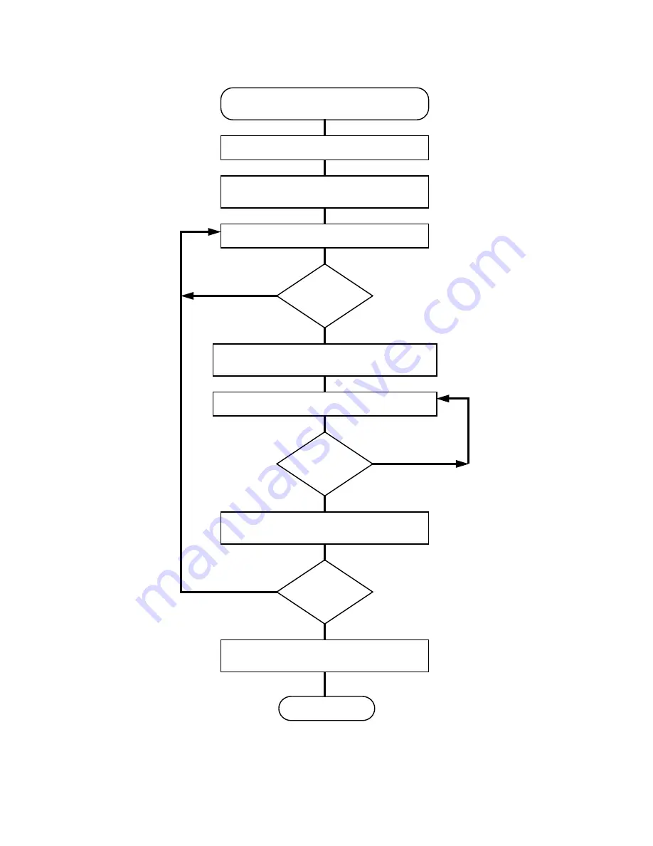
Figure 4.6.2-3.  Program Flowchart - Pipelined ADC Control Sequence

YES

NO

YES

NO

NO

YES

M3111/F4.6.2-3

READ LAST CHANNEL

Artisan Technology Group - Quality Instrumentation ... Guaranteed | (888) 88-SOURCE | www.artisantg.com

Summary of Contents for VMIVME-3111

Page 1: ...l service in house repair center WE BUY USED EQUIPMENT Sell your excess underutilized and idle used equipment We also offer credit for buy backs and trade ins www artisantg com WeBuyEquipment REMOTE INSPECTION Remotely inspect equipment before purchasing with our interactive website at www instraview com LOOKING FOR MORE INFORMATION Visit us on the web at www artisantg com for more information on ...

Page 2: ... MANUAL DOCUMENT NO 500 003111 000 T Revised June 19 1995 VME MICROSYSTEMS INTERNATIONAL CORPORATION 12090 SOUTH MEMORIAL PARKWAY HUNTSVILLE AL 35803 3308 205 880 0444 FAX NO 205 882 0859 1 800 322 3616 Artisan Technology Group Quality Instrumentation Guaranteed 888 88 SOURCE www artisantg com ...

Page 3: ... Factors 3 7 3 4 3 Interleaved Pipelined Operation 3 7 3 4 4 Programmable Gain Amplifier 3 8 3 5 FRONT PANEL P3 ANALOG INPUTS 3 8 3 5 1 P3 Low Pass Filters and Input Multiplexer 3 8 3 5 2 Current Loop Receiving Mode 3 8 3 6 REAR PANEL P2 ANALOG INPUTS 3 10 3 7 ANALOG INPUTS SIGNAL ROUTING 3 10 3 7 1 Self Test Multiplexer 3 10 3 7 2 Analog Configuration Network 3 13 3 8 ANALOG OUTPUTS 3 13 3 8 1 DA...

Page 4: ...S INTERRUPT CONTROL 4 25 4 9 1 Interrupt Control Register 4 26 4 9 2 Interrupt Vector Register 4 27 4 10 BOARD IDENTIFICATION REGISTER 4 28 SECTION 5 CONFIGURATION AND INSTALLATION 5 1 UNPACKING PROCEDURES 5 1 5 2 PHYSICAL INSTALLATION 5 1 5 3 BEFORE APPLYING POWER CHECKLIST 5 1 5 4 OPERATIONAL CONFIGURATION 5 2 5 4 1 Factory Installed Jumpers 5 2 5 4 2 Board Address and Address Modifier Selection...

Page 5: ...utocalibration 3 16 3 10 1 15 VDC Board Power 3 17 4 6 2 1 Program Flowchart Basic ADC Control Sequence 4 11 4 6 2 2 Program Example Basic ADC Control Sequence 4 12 4 6 2 3 Program Flowchart Pipelined ADC Control Sequence 4 13 4 6 2 4 Program Example Pipelined ADC Control Sequence 4 14 4 8 1 1 Program Flowchart Loopback Self Test 4 20 4 8 1 2 Program Example Loopback Self Test 4 21 4 8 2 1 Program...

Page 6: ...ing 4 16 4 7 1 1 DAC Data Format and Coding 4 18 4 8 2 1 Calibration Test Limits 4 22 4 9 1 Interrupt Registers 4 26 5 4 1 Programmable Jumper Functions 5 4 5 4 2 1 Typical Board Address FF8F00 HEX Selection 5 6 5 4 3 1 Voltage Range Configuration 5 7 5 6 1 P2 Connector Rear Panel Inputs Signal Assignments 5 16 5 6 2 P3 Connector Signal Assignments 5 18 APPENDIX A Schematic and Assembly Drawing Ar...

Page 7: ...under its patent rights or the rights of others For warranty and repair policies refer to VMIC s Standard Conditions of Sale AMXbus BITMODULE DMAbus MEGAMODULE NETbus SRTbus TESTCAL TURBOMODULE UCLIO UIOD VMEmanager VMEnet VMEnet II WARPNET and WinUIOC are trademarks of VME Microsystems International Corporation The VMIC logo and UIOC are registered trademarks of VME Microsystems International Cor...

Page 8: ... LIVE CIRCUITS Operating personnel must not remove product covers Component replacement and internal adjustments must be made by qualified maintenance personnel Do not replace components with power cable connected Under certain conditions dangerous voltages may exist even with the power cable removed To avoid injuries always disconnect power and discharge circuits before touching them DO NOT SERVI...

Page 9: ...ont panel analog input channels cable compatible with the 3V and 5V series signal conditioners c Two analog output channels with 10 mA drive capability d Program controlled off line operation of analog outputs e Resident 12 bit ADCs and DACs f Input and output ranges selectable as 0 to 5 V 0 to 10 V 2 5 V 5 V and 10 V g Optional low pass filters available for analog input noise elimination h ADC d...

Page 10: ...rate without degrading accuracy Two wideband analog outputs can supply 10 mA of drive current over the full output range of 10 V and can be operated off line for self test Built in Test BIT features permit off line verification of all active components by routing the analog outputs through the analog input multiplexers 1 3 REFERENCE MATERIAL LIST For a detailed explanation of the VMEbus and its ch...

Page 11: ... 10 mA 2 I O CONN P2 ADC DATA SETTLING DELAY GAIN TRACK CONV CMD CONV COMPL 12 S E ZERO GAIN 15 V OUTPUT MONITOR 2 12 DIFF PAIRS 15 LO HI HI LO LO ANALOG CONFIGURATION CONTROL STDS 10 V 4 DIFF PAIRS 1PAIR I O CONN P2 ANALOG INPUTS 32 PSEUDO DIFF RTN 16 DIFF PAIRS ANALOG INPUTS 16 I O CONN P3 GND SENSE 16 S E PIN COMPATIBLE WITH VMIC 3V 5V I O CABLES VME CONTROL BUS VMEbus CONN P1 Figure 1 2 1 VMIV...

Page 12: ...500 003111 000 2 1 SECTION 2 PHYSICAL DESCRIPTION AND SPECIFICATIONS REFER TO 800 003111 000 SPECIFICATION Artisan Technology Group Quality Instrumentation Guaranteed 888 88 SOURCE www artisantg com ...

Page 13: ...egories which are illustrated in the functional block diagram shown in Figure 1 2 1 All VMIVME 3111 functions are discussed in detail in subsequent sections of this manual a VMEbus Interface b Bus Interrupter c Analog Input Filters and Multiplexers d Analog Configuration Networks e Programmable Gain Amplifier f ADC Channel g Self Test Multiplexer h DACs i Analog Output Buffers and Switches j Autoc...

Page 14: ...devices on the board Address lines A01 through A04 map the 16 communication registers onto a 32 byte boundary within the VME address space Section 4 The control signals determine whether data is to be moved to the board WRITE or from the board READ The control signals also provide the necessary data strobes DS0 DS1 and supply a 16 MHz clock SYS CLK for use by on board timers A SYS RESET input rese...

Page 15: ...TOR A01 TO A04 4 DTACK SELECTION COMPARISON ADDRESS AND ADDRESS MODIFIER BOARD SELECTION COMPARATOR 21 A01 TO A15 AM0 TO AM5 VMEbus P1 SELECTION JUMPERS VME CONTROLS 5 WRITE DS0 DS1 SYS CLK SYS RESET 16 16 D00 TO D15 Figure 3 3 1 1 VMEbus Control Signals and Interface Logic M3111 F3 3 1 1 Artisan Technology Group Quality Instrumentation Guaranteed 888 88 SOURCE www artisantg com ...

Page 16: ... Settling Delay b Tracking Interval c Analog to Digital Conversion All ADC timing intervals discussed in this section are performed automatically by the on board smart controller Program control of the converter consists of basic handshake sequences The settling delay occurs directly after a state change has occurred in the analog networks such as selecting a new input channel and represents the s...

Page 17: ...RFACE LOGIC VMEbus IACK IACKIN WRITE SYSCLK A01 A02 A03 DATA RDY INT 0 IDB00 TO IDB07 8 DTACK 7 IRQ1 TO IRQ7 IRQ1 TO IRQ7 DTACK 7 Figure 3 3 2 1 Bus Interrupt Logic M3111 F3 3 2 1 VMEbus Artisan Technology Group Quality Instrumentation Guaranteed 888 88 SOURCE www artisantg com ...

Page 18: ...LK TIMER BUS TIMER RST SHORT SETTLING 4 TRACKING CONV CMD SYS CLK 16 MHz CONVERTER TIMING DECODE FROM ADC REGISTER CONTROL FROM CSR REGISTERED CONTROLS FROM CSR DECODED READ WRITE CONTROLS STATUS FLAGS TO CSR TO ADC Figure 3 4 1 ADC Timing Logic and Control Signals M3111 F3 4 1 Artisan Technology Group Quality Instrumentation Guaranteed 888 88 SOURCE www artisantg com ...

Page 19: ...channel N Number of channels T1 3111 settling delay 8 120 µs Gain x1 to x500 T2 3111 A D conversion time 19 µs T3 CPU controlling processor time invested per channel If CPU time is negligible relative to the conversion sequence then T3 is zero and the expression for maximum throughput N 1 is FT maximum 1 T1 T2 Maximum throughput for a gain of x1 then 37 037 samples per second for a single input ch...

Page 20: ...onfiguration network for selection into the ADC channel To achieve maximum system accuracy with filtered analog inputs the sample rate should be limited to 300 Hz or less per channel 4 8 kHz for 16 channels Higher sample rates will produce reflected pumpback currents at the inputs which can induce error voltages across the filter input resistors Each of the P3 analog inputs is selected by the four...

Page 21: ...500 003111 000 3 9 not exceeding 5 W Artisan Technology Group Quality Instrumentation Guaranteed 888 88 SOURCE www artisantg com ...

Page 22: ...L P3 INPUTS MUX A00 TO A04 15 SE CHANNEL SINGLE ENDED FILTERS 16 SE P3 ANALOG INPUTS CAL REFERENCE ANALOG OUTPUTS ANALOG COMMON 2 P3 CH 00 DIFF SE FILTERS 32 SE 16 DIFF ANALOG INPUTS P2 P2 CH 00 04 08 12 ANALOG TEST BUS 2 2 M3111 F3 5 1 Figure 3 5 1 Analog Inputs and Signal Routing Artisan Technology Group Quality Instrumentation Guaranteed 888 88 SOURCE www artisantg com ...

Page 23: ...ents Application programs therefore can realize the maximum sample rates permitted by the ADC timing controller 3 7 ANALOG INPUTS SIGNAL ROUTING After passing through the input multiplexers the analog input signals are routed to analog configuration networks for final switching into the ADC channel To test the input multiplexers four of the analog channels one for each multiplexer device are first...

Page 24: ...rors at the multiplexer inputs Operation of the self test multiplexer is described in detail later in this section and in Section 4 Artisan Technology Group Quality Instrumentation Guaranteed 888 88 SOURCE www artisantg com ...

Page 25: ...NDED OPERATION CH 00 HI CH 00 CH 00 LO CH 16 CH 15 HI CH 15 CH 15 LO CH 31 ANALOG COMMON TO MULTIPLEXERS FROM I O CONN Single ended channel M3111 F3 6 1 Figure 3 6 1 32 Channel Filtered Analog Inputs Artisan Technology Group Quality Instrumentation Guaranteed 888 88 SOURCE www artisantg com ...

Page 26: ... MULTIPLEXER A0 A1 P3 TEST 00 HI LO OUTPUT TEST 00 OUTPUT TEST 01 ANALOG COMMON SEL P3 TEST MULTIPLEXER EN ADDR DIFF ANALOG MUX DIFF ANALOG MULTIPLEXER ADDR EN ANALOG TEST BUS 2 2 2 2 2 2 2 2 Figure 3 7 1 Self Test Multiplexer M3111 F3 7 1 Artisan Technology Group Quality Instrumentation Guaranteed 888 88 SOURCE www artisantg com ...

Page 27: ...e range and for either bipolar or unipolar operation 3 8 2 Output Buffers and Switches Voltage levels from the DACs are buffered then switched to the P2 connector for routing through the system I O cables The output buffers are low leakage precision operational amplifiers which can supply 10 mA of drive current over the full available output voltage range of 10 V and which can withstand sustained ...

Page 28: ...ultiplexers This arrangement permits any one of the analog outputs to be sampled by the ADC It also verifies the operation of the analog input multiplexers by exercising them with known signal levels In addition to accepting the selected analog output signal the self test multiplexer permits the HIGH and LOW inputs of the Programmable Gain Amplifier PGA to be switched simultaneously to signal retu...

Page 29: ...ted by adjusting the reference input of the ADC The output of the 12 bit autogain DAC is offset and attenuated to produce a gain adjustment range of 1 2 percent which corresponds to an adjustment resolution of 0 0006 percent per DAC LSB Control data for the gain DAC is written as 12 bits right justified into a 16 bit WRITE ONLY register located at relative address 0A HEX in the VMIVME 3111 assigne...

Page 30: ...NP HI PGA INP LOW CONV CMD PROGRAMMABLE GAIN AMPLIFIER 12 bit ADC 12 bit R 2R LADDER CONVERTER INTERNAL REFERENCE ANALOG COMPARATOR CONTROL LOGIC CLOCK S A R CONV COMPL DIGITAL TRISTATE BUFFER 12 CONVERTER DATA INTERNAL DATA BUS RD CONV M3111 F3 9 4 1 Figure 3 9 4 1 Converter Channel Autocalibration Artisan Technology Group Quality Instrumentation Guaranteed 888 88 SOURCE www artisantg com ...

Page 31: ...00 3 19 DC TO DC CONVERTER 15 V ANA COM 15 V 5 V DIG GND 5 V GND VMEbus P1 M3111 F3 10 1 Figure 3 10 1 15 VDC Board Power Artisan Technology Group Quality Instrumentation Guaranteed 888 88 SOURCE www artisantg com ...

Page 32: ...SS MODE 00 02 04 06 08 0A 0C 0E 10 12 16 18 1A 1E 00 02 04 06 08 10 12 14 16 18 22 24 26 30 BOARD IDENTIFICATION CONTROL AND STATUS OUTPUT D A CHAN 00 OUTPUT D A CHAN 01 AUTOZERO D A CONV AUTOGAIN D A CONV A D CONVERTER DATA PGA GAIN SELECTION INTERRUPT CONTROL RESERVED INTERRUPT VECTOR RESERVED D08 D15 D00 D15 D00 D11 D00 D11 D00 D11 D00 D11 D00 D11 D00 D01 D00 D07 D00 D07 READ READ WRITE WRITE W...

Page 33: ...scribed in detail subsequently in the associated programming discussions Table 4 2 1 Control Register Functions CONTROL REGISTER DATA FORMAT MSB LSB D15 D14 D13 D12 D11 D10 D9 D8 D7 D6 D5 D4 D3 D2 D1 D0 0 1 1 1 0 0 1 0 0 1 0 0 0 0 0 0 CONTROL BIT NAME FUNCTION D0 MUX A0 H D1 MUX A1 H D0 through D4 select the analog input D2 MUX A2 H channel D3 MUX A3 H D4 MUX A4 H D5 BOARD RESET When D5 is HIGH 1 ...

Page 34: ...ime a 1 is written to this control bit D13 will be ignored if the Converter Data Register Table 4 1 1 contains unread data from a previous conversion The current settling sequence will be sustained until the Converter Data Register is READ D14 FAIL LED L The Fail LED is OFF if this bit is set to 1 and is ON if the bit is 0 D15 ENA EXT TRIG H If this bit is set it enables the P2 EXT TRIG L input si...

Page 35: ...g a 1 to the EN START CMD control bit causes the D13 flag to be set to 1 The flag will remain set until the next conversion has been completed and new data is available in the Converter Data Register The settling sequence will not run to completion if this flag is not set D14 D15 NEW DATA RDY When set to a 1 this flag indicates that a conversion has been completed and that data is available in the...

Page 36: ... a zero reference for the autozero operations P2 DIFFERENTIAL P2 input channels are configured as differential input pairs CSR control bits D0 through D3 select one of 16 input channels P3 inputs are configured as 16 single ended channels P2 SINGLE ENDED P2 input channels are configured as single ended inputs CSR control bits D0 through D4 select one of 32 input channels P3 inputs are configured a...

Page 37: ...trol of the following VMIVME 3111 Board parameters a Analog Input Mode b Channel Gain c Channel and Input Connector P2 P3 Selection The analog input mode is discussed in Section 4 4 Definition of the remaining channel selection board parameters is described in this section 4 5 1 Gain Selection Analog to Digital Converter ADC gain is program selectable as x1 x10 x100 or x500 The two least significa...

Page 38: ...analog inputs D7 1 or the rear panel P2 inputs D7 0 If the P3 inputs and control Mode 1 are selected then CSR control bits D0 through D3 select one of the 16 single ended inputs available at that connector P2 inputs can be configured as either differential or single ended channels In control Mode 1 the differential configuration is selected and CSR D0 through D4 selects one of 16 differential inpu...

Page 39: ...10 11 12 13 14 15 16 17 18 19 20 21 22 23 24 25 26 27 28 29 30 31 00 01 02 03 04 05 06 07 08 09 10 11 12 13 14 15 00 01 02 03 04 05 06 07 08 09 10 11 12 13 14 15 00 01 02 03 04 05 06 07 08 09 10 11 12 13 14 15 Table 4 5 2 1 Analog Input Channel Selection MODE D10 D9 D8 1 2 0 0 0 1 1 0 If P2 is configured with a combination of single ended and differential channels the single ended channels that ar...

Page 40: ... control approach permits the settling interval of a new channel to begin while a conversion is in progress This technique eliminates the settling interval from the throughput equation Section 3 and raises the throughput to approximately 59 kHz 4 6 1 ADC Timing All basic timing operations for the ADC are performed by the on board controller Control of the converter consists of the handshake progra...

Page 41: ...e written to the register simultaneously along with the operational mode and channel selections Figures 4 6 2 1 and 4 6 2 2 illustrate a measurement sequence which uses the basic conversion control method The sequence is simplified by the fact that only the NEW DATA RDY flag must be monitored in order to determine when each conversion has been completed The interleaved pipelined control method is ...

Page 42: ...TART CONVERSION SEQUENCE READ STATUS REGISTER NEW DATA READY LAST CHANNEL READ END SEQUENCE NO YES NO YES Figure 4 6 2 1 Program Flowchart Basic ADC Control Sequence M3111 F4 6 2 1 SET PGA GAIN SELECTION READ NEW DATA Artisan Technology Group Quality Instrumentation Guaranteed 888 88 SOURCE www artisantg com ...

Page 43: ... PGA GAIN SELECTION REG CONTROL STATUS REG A D CONVERTER DATA REG DATA STORAGE ADDRESS CONTROL WORD CH 00 CONTROL WORD CH 31 SELECT GAIN X1 WRITE CONTROL WORD READ STATUS REG IS NEW DATA READY IF NOT CHECK AGAIN READ AND STORE DATA LAST CHANNEL READ IF SO END SEQUENCE GET NEXT CONTROL WORD DO NEXT CHANNEL M3111 F4 6 2 2 Figure 4 6 2 2 Program Example Basic ADC Control Sequence Artisan Technology G...

Page 44: ...USY START CONVERSION WAIT FOR CONV BUSY SELECT NEXT CHANNEL START SETTLING READ STATUS REGISTER DATA READY READ DATA REGISTER STORE DATA IN MEMORY LAST CHANNEL SELECTED END SEQUENCE Figure 4 6 2 3 Program Flowchart Pipelined ADC Control Sequence YES NO YES NO NO YES M3111 F4 6 2 3 READ LAST CHANNEL Artisan Technology Group Quality Instrumentation Guaranteed 888 88 SOURCE www artisantg com ...

Page 45: ...L STATUS REG A D CONVERTER DATA REG DATA STORAGE ADDRESS CONTROL WORD CH 00 CONTROL WORD CH 31 CONTROL WORD CONVERT SELECT GAIN X1 WRITE CONTROL WORD READ STATUS REG IS SETTLING BUSY IF SO CHECK AGAIN START CONVERSION SELECT NEXT CHANNEL SELECT NEXT CHANNEL START SETTLING THAT CHANNEL READ STATUS REG IS NEW DATA READY HIGH IF NOT CHECK AGAIN READ AND STORE DATA LAST CHANNEL READ IF SO END SEQUENCE...

Page 46: ...major points within the full scale ranges shown For any offset binary converter output code BIPOLAR RANGE the associated input voltage is obtained with the expression INPUT Volts EFSR 2 EFSR x DECIMAL OUTPUT CODE 4096 x GAIN where EFSR is the full scale range voltage e g EFSR 10 Volts for the 5 V range and gain is the program selected gain of the Programmable Gain Amplifier PGA The input voltage f...

Page 47: ...00 V 0 0049 V 0 0000 V 9 9951 V 10 0000 V 4 9976 V 2 5000 V 0 0024 V 0 0000 V 4 9976 V 5 0000 V 0000 0000 0000 0000 0000 0000 1111 1100 1000 1000 0000 0000 1111 0000 0000 0000 0000 0000 1111 0000 0001 0000 0001 0000 BIPOLAR RANGES TWO S COMPLEMENT INPUT 10 V 5 V D15 D0 FS 1 LSB 1 2 FS 1 LSB ZERO 1 LSB FS 1 LSB FS 9 9951 V 5 0000 V 0 0049 V 0 0000 V 0 0049 V 9 9951 V 10 0000 V 0000 0000 0000 0000 1...

Page 48: ... return P2 pin C28 to the board ground For location of the jumpers refer to Section 5 Figure 5 4 1 Be aware that the P2 I O pins are sometimes used by other boards to perform different I O functions From a systems viewpoint verify that multiple drivers receivers are not using these user defined P2 I O lines P2 A28 and P2 C28 4 7 CONTROLLING THE ANALOG OUTPUTS The analog output channels on the VMIV...

Page 49: ...00 1111 0000 0001 0000 0001 0000 4 9976 V 2 5000 V 0 0024 V 0 0000 V 4 9976 V 5 0000 V M3111 T4 7 1 1 x Don t care 4 7 2 Off Line Operation Setting the OUTPUT ON LINE control bit HIGH Table 4 2 1 connects the analog outputs to the P2 I O connector for normal system cooperation Clearing the bit LOW disconnects the analog outputs from P2 However the output buffers can still be monitored through the ...

Page 50: ...her the ANALOG OUTPUT CHAN 00 or the ANALOG OUTPUT CHAN 01 in the analog input mode shown in Table 4 4 1 The selected output channel can then be exercised by the controlling processor and monitored by the VMIVME 3111 ADC to verify that all components in the loopback signal path are operating correctly This technique is illustrated in Figures 4 8 1 1 and 4 8 1 2 Artisan Technology Group Quality Ins...

Page 51: ...AGE TO OUTPUT CHANNEL MIN 50 µs DELAY START READ ADC COMPARE ADC READING WITH OUTPUT TEST VOLTAGE COMPARE WITHIN TEST LIMITS SET LOOPBACK TEST FAIL FLAG LAST DATA END SEQUENCE SELECT NEXT OUTPUT DATA YES NO NO YES Figure 4 8 1 1 Program Flowchart Loopback Self Test M3111 F4 8 1 1 Artisan Technology Group Quality Instrumentation Guaranteed 888 88 SOURCE www artisantg com ...

Page 52: ...SELECT GAIN X1 CLEAR LOOPBACK FAIL FLAG CONTROL WORD D A CH 00 CLEAR DATA REGISTER ADDRESS CHANNEL 00 WRITE DATA OUT SET DELAY DELAY END DELAY WRITE CONTROL WORD READ STATUS REGISTER IS NEW DATA READY IF NOT CHECK AGAIN READ NEW DATA SUBTRACT WRITE FROM READ IF POS TRUE DON T NEGATE NEGATE NEG TRUE TO POS TRUE COMPARE TO MAX ERROR VALUE FAIL IF MAX ERROR VALUE INCREMENT DATA REGISTER DONE ALL DATA...

Page 53: ...gs Table 4 8 2 1 Calibration Test Limits NOMINAL SELF TEST STANDARD VDC REFERENCE VOLTAGE VDC FULL SCALE RANGE VDC ACCEPTANCE RANGE HEX 0 LSB NOMINAL 2 LSB MAX MIN 4 LSB MAX MIN 10 0 5 0 2 5 ZERO ZERO 2 5 5 0 10 0 9 9512 4 9756 2 4878 0 0000 0 0000 2 4878 4 9756 9 9512 0 TO 10 10 0 TO 5 5 2 5 ALL BIPOLAR RANGES ALL UNIPOLAR RANGES 2 5 5 10 0FEC 0FF6 0FEC 0FF6 0FEC 0800 0000 000A 000A 000A 0FEE 0FF...

Page 54: ...RE TO CORRECT VALUE IS ERROR NOW NEGATIVE LSB OF CORRECTION REGISTER CHECKED CLEAR THIS BIT NO YES NO YES SET NEXT BIT IN GAIN CALIBRATION DAC DELAY DO CONVERSION OF POS TEST REF AND STORE THE READING COMPARE TO CORRECT VALUE IS ERROR NOW NEGATIVE LSB OF CORRECTION REGISTER CHECKED CLEAR THIS BIT NO YES NO DECREMENT BIT COUNTER DECREMENT BIT COUNTER SET BIT COUNTER TO START Artisan Technology Grou...

Page 55: ...T THE BIT COUNTER IF BIT COUNTER 0 CALGAIN DO CAL ZERO WITHOUT DOING CAL GAIN ON THE LAST PASS SET THE BIT COUNTER START SELECT P G A GAIN X1 SET NEXT ERROR CORRECT BIT WRITE ERROR CORRECTION REG SELECT POSITIVE TEST REF DO ADC READING SUBROUTINE COMPARE TO EXPECTED READING IF GAIN CALLED THEN DO ENDSEQ IF ERROR POSITIVE CONTINUE IF ERROR NEGATIVE CLR BIT DECREMENT THE BIT COUNTER IF BIT COUNTER 0...

Page 56: ... To eliminate the requirement for polling the VMIVME 3111 board during basic conversion sequencing the VMIVME 3111 board is equipped to provide an interrupt at the end of each conversion sequence The interrupt response is established through the INTERRUPT CONTROL and INTERRUPT VECTOR Registers Table 4 6 2 1 which are described in the following paragraphs During BOARD RESET or SYSTEM RESET the Inte...

Page 57: ...7 D6 D5 D4 D3 D2 D1 D0 LSB D8 TO D15 NOT USED V7 V6 V5 V4 V3 V2 V1 V0 INTERRUPT VECTOR M3111 T4 9 1 4 9 1 Interrupt Control Register The Interrupt Control Register Table 4 9 1 controls the interrupt level as well as the enabling or disabling of the interrupt The function of each register bit is described in the following definitions Artisan Technology Group Quality Instrumentation Guaranteed 888 8...

Page 58: ...o the request The IRE bit must then be set HIGH again to enable the interrupt EXTERNAL INTERNAL X IN Bit 5 This control bit has no valid function on the VMIVME 3111 board and MUST be cleared LOW at all times FLAG F Bit 7 This control bit has no affect on the operation of the VMIVME 3111 board and is available for use by the controlling processor as a utility flag FLAG AUTO CLEAR FAC Bit 6 If FAC i...

Page 59: ...n identification of the board or as an address vector 4 10 BOARD IDENTIFICATION REGISTER By reading the Board Identification Register located at address 00 Table 4 6 2 1 an 8 bit left justified identification code of 0D will be obtained from the VMIVME 3111 board Artisan Technology Group Quality Instrumentation Guaranteed 888 88 SOURCE www artisantg com ...

Page 60: ...rd s should be checked for broken components damaged circuit board s heat damage and other visible contamination All claims arising from shipping damage should be filed with the carrier and a complete report sent to VMIC together with a request for advice concerning the disposition of the damaged item s 5 2 PHYSICAL INSTALLATION CAUTION DO NOT INSTALL OR REMOVE THE BOARDS WHILE THE POWER IS APPLIE...

Page 61: ...rocessing unit CAUTION DO NOT INSTALL OR REMOVE THIS BOARD WITH POWER APPLIED TO THE SYSTEM 5 4 OPERATIONAL CONFIGURATION Control of the VMIVME 3111 board address and I O Access Mode are determined by field replaceable on board jumpers This section describes the use of these jumpers and their effects on board performance The locations and functions of all VMIVME 3111 jumpers are shown in Figure 5 ...

Page 62: ...6 J40 J38 J35 3 1 J4 J5 3 1 J15 J13 J12 J3 J2 3 1 3 1 3 1 P3 U1 J8 J9 J7 J11 J10 J24 J23 J34 J33 J22 J21 J32 J31 J20 J19 J30 J29 J18 J17 J28 J27 J39 M3111 F5 4 1 Figure 5 4 1 Jumper Locations J1 J41 J42 3 1 Artisan Technology Group Quality Instrumentation Guaranteed 888 88 SOURCE www artisantg com ...

Page 63: ...03 19 SINGLE ENDED P2 CHAN 04 20 SINGLE ENDED P2 CHAN 05 21 SINGLE ENDED P2 CHAN 06 22 SINGLE ENDED P2 CHAN 07 23 SINGLE ENDED P2 CHAN 08 24 SINGLE ENDED P2 CHAN 09 25 SINGLE ENDED P2 CHAN 10 26 SINGLE ENDED P2 CHAN 11 27 SINGLE ENDED P2 CHAN 12 28 SINGLE ENDED P2 CHAN 13 29 SINGLE ENDED P2 CHAN 14 30 SINGLE ENDED P2 CHAN 15 31 SINGLE ENDED INSTALLED INSTALLED INSTALLED INSTALLED INSTALLED INSTALL...

Page 64: ... GAIN ADJUST AUTO INPUT GAIN ADJUST UNIPOLAR ANALOG OUTPUTS BIPOLAR ANALOG OUTPUTS 10 V FSR ANALOG OUTPUTS 5 V FSR ANALOG OUTPUTS GROUND ANALOG OUTPUTS RETURN CONNECTS EXT TRIG TO P2 GND SENSE CONNECTS TRIG RTN TO P2 GND SENSE CONNECTS TRIG RTN TO GROUND INSTALLED INSTALLED INSTALLED OPTION OPTION INSTALLED OMITTED OMITTED OMITTED OMITTED INSTALLED OMITTED INSTALLED OMITTED INSTALLED OMITTED OMITT...

Page 65: ...the shorting plugs at the one or HIGH positions Address bit A05 has a weight of 32 byte locations As an example the jumper arrangement shown in Table 5 4 2 1 would produce a board address of XXXX8F00 HEX Address bits XXXX are CPU dependent I O ACCESS MODE is programmed by selecting the value of the address modifier bit AM2 with jumper J37 3 Short nonprivileged access is selected by installing the ...

Page 66: ... jumper J2 is installed and enabled if J2 is removed 5 4 4 Current Loop Termination Resistors The low pass input filter capacitors are replaced with 250 Ω 0 02 percent precision resistors when the board is equipped with the current loop termination option 5 4 5 Differential Single Ended Input Mode Selection All P3 analog inputs are single ended channels The P2 analog inputs however can be jumper p...

Page 67: ...resealed with a suitable fast curing sealing compound after recalibration has been completed 5 5 1 Equipment Required a Digital Voltmeter DVM 1 000 VDC and 10 000 VDC ranges five or more digits 0 005 percent of voltage range measurement accuracy 10 MΩ minimum input impedance b Digital Voltage Source Voltage Input Option Only 1 000 VDC and 10 000 VDC output voltage ranges 0 005 percent of range acc...

Page 68: ...P1 P2 U15 U52 U3 U51 P3 U1 M3111 F5 5 1 Figure 5 5 1 Test Point and Adjustment Locations R59 R35 R36 TP5 R66 R60 R61 R62 R87 R27 R25 TP4 TP1 TP2 Artisan Technology Group Quality Instrumentation Guaranteed 888 88 SOURCE www artisantg com ...

Page 69: ...oltage Input Option Calibration a Connect the positive lead of the digital voltage source to Pin A1 of P2 Jumper Pins A1 and C1 of P2 together Connect the negative lead of the voltage source to Pin A2 of P2 Place the J38 jumper in the J38 1 2 MAN ZERO position b Connect the positive lead of the DVM to test point TP4 T H INPUT and the negative lead to the test point TP1 SIG RTN c Select the Self Te...

Page 70: ...DC 5 5 3 2 Current Input Option Calibration a Adjust the current source output to 0 0 mA Connect the positive lead of the current source to Pin A1 of P2 Connect the negative lead of the current source to Pin C2 of P2 Place the J38 jumper in the J38 1 2 MAN ZERO position Install jumper J24 b Connect the positive lead of the DVM to test point TP4 T H INPUT and the negative lead to the testpoint TP1 ...

Page 71: ... V REF REMOVED J26 10 V REF INSTALLED J40 5 V REF REMOVED J38 1 2 MANUAL ZERO INSTALLED J6 UNIPOLAR REMOVED b Select a PGA gain of x1 by writing 0000 to the PGA gain selection register Select the SELF TEST ZERO input and initiate A D conversions by writing 6040 HEX to the CSR at intervals of 0 1 1 0 second Display the ADC register after each conversion c Adjust R25 BIPOLAR ADC ZERO ADJ for an ADC ...

Page 72: ...he DVM to Pin A31 of P2 Adjust R35 ANA CH 0 GAIN ADJ for a DVM indication of 10 000 0 002 VDC i Establish positive full scale outputs by writing 0FFF HEX to the output DAC Registers Verify that the output levels on pins A31 and A32 of P2 are 9 995 0 004 VDC j Calibration is completed Remove all test connections Remove power Restore all board jumpers to their original locations 5 6 CONNECTOR DESCRI...

Page 73: ...nection to the 3V 5V series of nonmultiplexed voltage output signal conditioner assemblies Remote sensing of the 3V 5V assembly signal return is established on the VMIVME 3111 board by removing the J39 jumper NOTE IF P2 OR P3 IS CONFIGURED FOR CURRENT LOOP TERMINATION THE INPUT RESISTANCE OF EACH CHANNEL WILL BE VERY LOW AND WILL PRODUCE SIGNIFICANT LOADING OF VOLTAGE INPUTS EXCESSIVE HEATING AND ...

Page 74: ...3 PIN 14 PIN 15 PIN 16 PIN 17 PIN 18 PIN 19 PIN 20 PIN 21 PIN 22 PIN 23 PIN 24 PIN 25 PIN 26 PIN 27 PIN 28 PIN 29 PIN 30 PIN 31 PIN 32 REAR VIEW OF BOARD PC BOARD M3111 F5 6 1 Figure 5 6 1 P2 Connector Pin Configuration Artisan Technology Group Quality Instrumentation Guaranteed 888 88 SOURCE www artisantg com ...

Page 75: ...D SEN CH 28 GND SEN CH 29 TRIG RTN CH 30 CH 31 DIFFERENTIAL INPUTS CH 00 HI GND SEN CH 01 HI GND SEN CH 02 HI GND SEN CH 03 HI GND SEN CH 04 HI GND SEN CH 05 HI GND SEN CH 06 HI GND SEN CH 07 HI GND SEN CH 08 HI GND SEN CH 09 HI GND SEN CH 10 HI GND SEN CH 11 HI GND SEN CH 12 HI GND SEN CH 13 HI EXT TRIG CH 14 HI CH 15 HI ROW A SIGNAL ROW C SIGNAL CH 00 LO GND SEN CH 01 LO GND SEN CH 02 LO GND SEN...

Page 76: ...111 000 5 17 26 25 PC BOARD FRONT VIEW OF CONNECTOR 2 PIN 1 M3111 F5 6 2 Figure 5 6 2 P3 Connector Pin Configuration Artisan Technology Group Quality Instrumentation Guaranteed 888 88 SOURCE www artisantg com ...

Page 77: ...8 19 20 21 22 23 24 25 26 CHAN 00 CHAN 08 RETURN CHAN 09 CHAN 01 RETURN CHAN 02 CHAN 10 RETURN CHAN 11 CHAN 03 RETURN CHAN 04 CHAN 12 RETURN CHAN 13 CHAN 05 RETURN CHAN 06 CHAN 14 RETURN CHAN 15 CHAN 07 RETURN GND SENSE NO CONN M3111 T5 6 2 Artisan Technology Group Quality Instrumentation Guaranteed 888 88 SOURCE www artisantg com ...

Page 78: ...ns are clean and free from contamination g No components of adjacent boards are disturbed when inserting or removing the board from the chassis h Quality of cables and I O connections If the products must be returned contact VMIC for a Return Material Authorization RMA Number This RMA Number must be obtained prior to any return 6 2 MAINTENANCE PRINTS User level repairs are not recommended The appe...

Page 79: ...APPENDIX A SCHEMATIC AND ASSEMBLY DRAWING Artisan Technology Group Quality Instrumentation Guaranteed 888 88 SOURCE www artisantg com ...

Page 80: ...l service in house repair center WE BUY USED EQUIPMENT Sell your excess underutilized and idle used equipment We also offer credit for buy backs and trade ins www artisantg com WeBuyEquipment REMOTE INSPECTION Remotely inspect equipment before purchasing with our interactive website at www instraview com LOOKING FOR MORE INFORMATION Visit us on the web at www artisantg com for more information on ...

Reviews: