background image

The module is powered by 

single power supply

, use 3.3 V or +5 V 

on appropriate pin 13 or 15.
All module inputs are LVTTL and are 5 V tolerant.
Outputs pins with names prefixed by dash character ("-") are active in log. 0, 

all other signals are active in log. 1.
All   outputs   are   doubled.   Outputs   on   pins   5   to   8   are   with   3.3 V   levels   and 

connect directly ENC28J60. If 5 V power supply is used, signals with 5 V levels 

are available on pins 1 to 4. Connect outputs with corresponding voltage level 

according to applications need, see the table above.

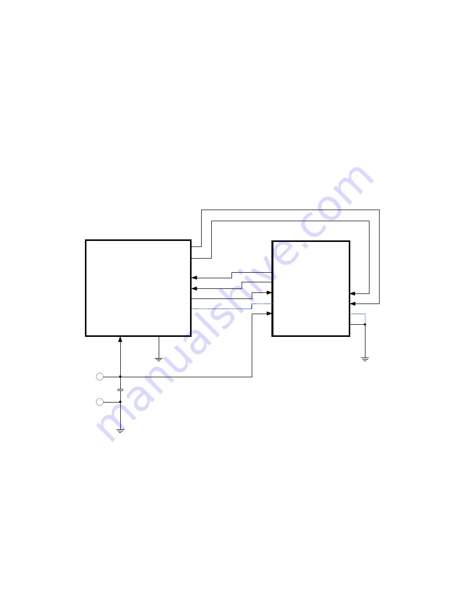
2.1 Connection to 3.3 V application

If the modules is to be used in 3.3 V application input and output signals of 

ENC28J60 are used directly.

-INT5
SO5
-INT
SO
SCK
-RST
+3V3
+5V

CLKO5

-WOL5

CLKO

-WOL

SI

-CS

GND
GND

uPC

MSEL

MOSI

-INT1
-INT0

MISO

MCLK

VDD       GND

GND

+3V3

100nF

SPINET

3,3V application

2.2 Connection to 5 V application

In case the module is to be used in 5 V application, the output signals are 

connected   through   integrated   level   converter   while   input   signals   are   are 

connected directly ENC28J60 (which is 5 V tolerant). A 3.3 V voltage regulator 

for powering the ENC28J60 is part of the module.

Page 4

Summary of Contents for SPINET

Page 1: ...sted checksum calculation Power by 3 3 V or 5 V Outputs with both 3 3 V and 5 V levels 5 V tolerant inputs Easy connection to PVK40 board Example program in C Address ASIX s r o Staropramenna 4 150 00 Prague Czech Republic E Mail info asix tools com general information sales asix tools com sales inquiries ordering support asix tools com technical support WWW www asix tools com development tools ww...

Page 2: ... 6 5 MECHANICAL DESIGN 7 6 TECHNICAL SPECIFICATIONS 8 6 1 Recommended values for 3 3 V application 8 6 2 Recommended values for 5 V application 8 Note This document contains hyperlinks pointing to web pages on the Internet If the links happen to be broken pointing to a non existing page please download recent version of this manual from www asix tools com Page 2 ...

Page 3: ...ides of other features it includes hardware engine for copying blocks of memory and checksum calculation in one s complement arithmetics IP checksum and CRC 2 INPUTS AND OUTPUTS Pin Label Type Description 3 3 V 5 V 1 INT5 OUT Interrupt pin 2 CLKO5 OUT User clock output 3 SO5 OUT Serial data out 4 WOL5 OUT Wake On LAN 5 INT OUT Interrupt pin 6 CLKO OUT User clock output 7 SO OUT Serial data out 8 W...

Page 4: ...ing voltage level according to applications need see the table above 2 1 Connection to 3 3 V application If the modules is to be used in 3 3 V application input and output signals of ENC28J60 are used directly INT5 SO5 INT SO SCK RST 3V3 5V CLKO5 WOL5 CLKO WOL SI CS GND GND uPC MSEL MOSI INT1 INT0 MISO MCLK VDD GND GND 3V3 100nF SPINET 3 3V application 2 2 Connection to 5 V application In case the...

Page 5: ...turer A suitable MAC address shall be assigned to the module during startup configuration of ENC28J60 If yo are not assigned Organization unique identifier OUI by IEEE it is recommended to use an address from locally administered range that is an address with bit 1 second least significant in its first byte set e g 02 00 00 00 00 78 Note The module provides with solution of communication over Ethe...

Page 6: ...4 ELECTRICAL SCHEMATICS Page 6 ...

Page 7: ...5 MECHANICAL DESIGN SPINET all dimensions in millimeters Page 7 Ø 3 8 48 57 5 11 35 40 ...

Page 8: ...x 200 mA Input voltage log 1 VIH min 2 25 V max 5 5 V Input voltage log 0 VIL max 1 V Output voltage log 1 5 V VOH5 min 4 4 V Output voltage log 0 5 V VOL5 max 0 1 V Output pin current 5 V Iout5 max 25 mA Values for use in other than typical environment are available in datasheets for ENC28J60 74AHCT541 and LF33 Page 8 SPINET_EN Copyright 1991 2007 ASIX s r o All trademarks used in this document a...

Reviews: