background image


Chapter 2 

 Hardware Information 


16


EPIC
 Bo

ar

d  


EPIC
-C

FS

7-

PUC


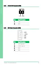
2.4.4 

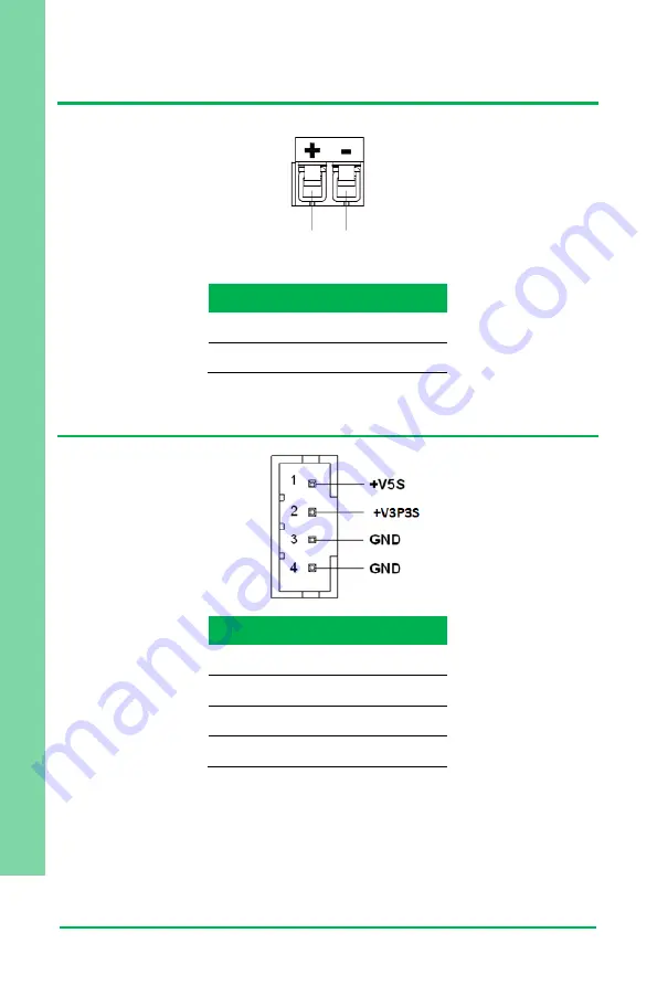
2 Pin DC IN Connector (CN5) 


Pin 

Signal Description 

+12V 

GND 


2.4.5 

DIO Power Connector (CN6) 


Pin 

Signal Description 

+V5S max 0.5A 

+V3P3S max 1A 

GND 

GND 


+VIN GND

Summary of Contents for Aaeon EPIC-CFS7-PUC

Page 1: ...Last Updated May 6 2021 EPIC CFS7 PUC EPIC Board User s Manual 1st Ed ...

Page 2: ...n this manual is intended to be accurate and reliable However the original manufacturer assumes no responsibility for its use or for any infringements upon the rights of third parties that may result from its use The material in this document is for product information only and is subject to change without notice While reasonable efforts have been made in the preparation of this document to assure...

Page 3: ...s not specifically named in this section Microsoft Windows is a registered trademark of Microsoft Corp Intel Pentium and Celeron are registered trademarks of Intel Corporation Intel Core and Intel Atom are trademarks of Intel Corporation ITE is a trademark of Integrated Technology Express Inc IBM PC AT PS 2 and VGA are trademarks of International Business Machines Corporation All other product nam...

Page 4: ...setting up your product please make sure the following items have been shipped Item Quantity EPIC CFS7 PUC 1 Jumper Cap 1 Back plate for cooler 1 If any of these items are missing or damaged please contact your distributor or sales representative immediately ...

Page 5: ...escriptions and explanations on the product s hardware and software features if any its specifications dimensions jumper connector settings definitions and driver installation instructions if any to facilitate users in setting up their product Users may refer to the product page at AAEON com for the latest version of this document ...

Page 6: ...nsient over voltage 7 Always disconnect this device from any AC supply before cleaning 8 While cleaning use a damp cloth instead of liquid or spray detergents 9 Make sure the device is installed near a power outlet and is easily accessible 10 Keep this device away from humidity 11 Place the device on a solid surface during installation to prevent falls 12 Do not cover the openings on the device to...

Page 7: ...on to the device iii Exposure to moisture iv Device is not working as expected or in a manner as described in this manual v The device is dropped or damaged vi Any obvious signs of damage displayed on the device 18 DO NOT LEAVE THIS DEVICE IN AN UNCONTROLLED ENVIRONMENT WITH TEMPERATURES BEYOND THE DEVICE S PERMITTED STORAGE TEMPERATURES SEE CHAPTER 1 TO PREVENT DAMAGE ...

Page 8: ...sion if the battery is incorrectly replaced Replace only with the same or equivalent type recommended by the manufacturer Dispose of used batteries according to the manufacturer s instructions and your local government s recycling or disposal directives Attention Il y a un risque d explosion si la batterie est remplacée de façon incorrecte Ne la remplacer qu avec le même modèle ou équivalent recom...

Page 9: ...铅 Pb 汞 Hg 镉 Cd 六价铬 Cr VI 多溴联苯 PBB 多溴二苯 醚 PBDE 印刷电路板 及其电子组件 外部信号 连接器及线材 外壳 中央处理器 与内存 硬盘 液晶模块 光驱 触控模块 电源 电池 本表格依据 SJ T 11364 的规定编制 表示该有毒有害物质在该部件所有均质材料中的含量均在 GB T 26572标准规定的限量要求以下 表示该有害物质的某一均质材料超出了GB T 26572的限量要求 然而该部件 仍符合欧盟指令2011 65 EU 的规范 备注 一 此产品所标示之环保使用期限 系指在一般正常使用状况下 二 上述部件物质中央处理器 内存 硬盘 光驱 电源为选购品 三 上述部件物质液晶模块 触控模块仅一体机产品适用 ...

Page 10: ...SU X O O O O O Battery X O O O O O This form is prepared in compliance with the provisions of SJ T 11364 O The level of toxic or hazardous materials present in this component and its parts is below the limit specified by GB T 26572 X The level of toxic of hazardous materials present in the component exceed the limits specified by GB T 26572 but is still in compliance with EU Directive 2011 65 EU R...

Page 11: ...Board 13 2 4 1 LPC Port CN1 14 2 4 2 SATA Connector CN2 15 2 4 3 SATA Power CN4 15 2 4 4 2 Pin DC IN Connector CN5 16 2 4 5 DIO Power Connector CN6 16 2 4 6 PCIe x4 FPC Connector CN9 17 2 4 7 CPU FAN Connector CN10 18 2 4 8 POE LAN RJ 45 Connector CN11 18 2 4 9 RS232 422 485 connector COM1 COM2 CN12 13 19 2 4 10 HDMI Connector CN14 15 21 2 4 11 USB 3 2 Gen 2 Connector CN16 22 2 4 12 USB 3 2 Gen 2 ...

Page 12: ... DIO Board 32 2 7 1 LPC Port CN1 32 2 7 2 Power In CN2 33 2 7 3 GPI Port CN3 34 2 7 4 GPO Port CN4 35 2 8 Block Diagrams 37 Chapter 3 BIOS Setup 39 3 1 System Test and Initialization 40 3 2 AMI BIOS Setup 41 3 3 Setup Submenu Main 42 3 4 Setup Submenu Advanced 43 3 4 1 CPU Configuration 44 3 4 2 SATA Configuration 45 3 4 3 Hardware Monitor 46 3 4 3 1 Smart Fan Mode Configuration 47 3 4 4 SIO Confi...

Page 13: ...ty 58 3 6 1 Secure Boot 59 3 6 1 1 Key Management 60 3 7 Setup Submenu Boot 62 3 7 1 BBS Priorities 63 3 8 Setup Submenu Save Exit 64 Chapter 4 Driver Installation 65 4 1 Driver Installation 66 Appendix A I O Information 68 A 1 I O Address Map 69 A 2 Memory Address Map 72 A 3 IRQ Mapping Chart 73 Appendix B Watchdog Timer Programming 75 B 1 Watchdog Timer Registers 76 B 2 Watchdog Sample Program 7...

Page 14: ...EPIC Board EPIC CFS7 PUC Chapter 1 Chapter 1 Product Specifications ...

Page 15: ...annel Non ECC Max Memory Capacity Up to 32GB BIOS AMI UEFI Wake on LAN Yes Watchdog Timer 255 Levels Power Requirement 12V Power Supply Type AT ATX Power Consumption Typical 95 04W system Dimensions System L x W x H 8 50 x 7 09 x 2 56 216mm x 180mm x 65mm Board L x W 4 53 x 6 5 115mm x 165mm Operating Temperature 32 F 122 F 0 C 50 C Storage Temperature 4 F 176 F 20 C 80 C Operating Humidity 0 90 4...

Page 16: ... two ports on main board two ports on daughter board Audio USB Port USB3 2 Gen 2 USB2 0 x 4 Rear I O USB2 0 x 2 Internal header Serial Port RS 232 422 485 x 2 Internal header Parallel Port printer port HDD Interface SATA III 6 0 Gbps x 1 SSD Expansion Slot PCIe x4 FPC slot For PoE card Full Size mSATA mPCIe slot x 1 LPC Bus SMBus default I2C option DIO Isolated DIO 32 bits 16 bits in 16 bits out s...

Page 17: ...4 EPIC Board EPIC CFS7 PUC Chapter 2 Chapter 2 Hardware Information ...

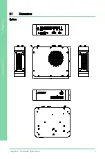
Page 18: ...Chapter 2 Hardware Information 5 EPIC Board EPIC CFS7 PUC 2 1 Dimensions System ...

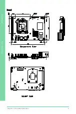
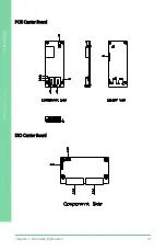
Page 19: ...Chapter 2 Hardware Information 6 EPIC Board EPIC CFS7 PUC Board ...

Page 20: ...Chapter 2 Hardware Information 7 EPIC Board EPIC CFS7 PUC POE Carrier Board DIO Carrier Board ...

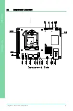
Page 21: ...Chapter 2 Hardware Information 8 EPIC Board EPIC CFS7 PUC 2 2 Jumpers and Connectors ...

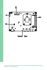
Page 22: ...Chapter 2 Hardware Information 9 EPIC Board EPIC CFS7 PUC ...

Page 23: ...Chapter 2 Hardware Information 10 EPIC Board EPIC CFS7 PUC POE Carrier Board DIO Carrier Board ...

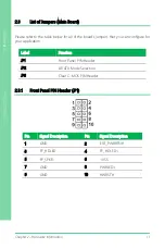
Page 24: ...l of the board s jumpers that you can configure for your application Label Function JP1 Front Panel PIN Header JP2 AT ATX Mode Selection JP3 Clear C MOS PIN Header 2 3 1 Front Panel PIN Header JP1 Pin Signal Description Pin Signal Description 1 GND 2 EXT_PWRBTN 3 FP_HDLED 4 FP_HDLED 5 FP_SPKR 6 V5S 7 GND 8 PWRLED 9 GND 10 HWRST ...

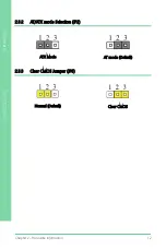
Page 25: ...Chapter 2 Hardware Information 12 EPIC Board EPIC CFS7 PUC 2 3 2 AT ATX mode Selection JP2 ATX Mode AT mode Default 2 3 3 Clear CMOS Jumper JP3 Normal Default Clear CMOS ...

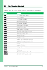
Page 26: ...ector CN5 2 Pin DC IN Connector CN6 DIO Power Connector CN9 PCIe x4 FPC Connector CN10 CPU Fan Connector CN11 POE LAN RJ45 Connector CN12 RS232 422 485 COM2 Connector CN13 RS232 422 485 COM1 Connector CN14 HDMI Connector CN15 HDMI Connector CN16 USB 3 2 Gen 2 10 Gbps Connector CN17 USB 3 2 Gen 2 10 Gbps Connector CN18 RTC Connector CN19 USB 2 0 Connector CN20 Mini Card Connector CPU1 CPU Socket DI...

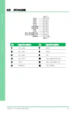
Page 27: ...ation 14 EPIC Board EPIC CFS7 PUC 2 4 1 LPC Port CN1 Pin Signal Description Pin Signal Description 1 LPC_AD0 7 RST 2 LPC_AD1 8 GND 3 LPC_AD2 9 CLK 4 LPC_AD3 10 I2C0_data SMB_data 5 P3V3 11 I2C0_CLK SMB_CLK 6 FRAME 12 INT_SERIRQ ...

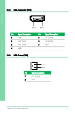
Page 28: ...C Board EPIC CFS7 PUC 2 4 2 SATA Connector CN2 Pin Signal Description Pin Signal Description 1 GND 5 SATA_RXN0 2 SATA_TXP0 6 SATA_RXP0 3 SATA_TXN0 7 GND 4 GND 2 4 3 SATA Power CN4 Pin Signal Description 1 5V max 1A 2 GND Pin 1 Pin 7 5V GND ...

Page 29: ...dware Information 16 EPIC Board EPIC CFS7 PUC 2 4 4 2 Pin DC IN Connector CN5 Pin Signal Description 1 12V 2 GND 2 4 5 DIO Power Connector CN6 Pin Signal Description 1 V5S max 0 5A 2 V3P3S max 1A 3 GND 4 GND VIN GND ...

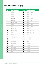
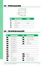
Page 30: ... 23 GND 4 SMB_DATA 24 PCIE_11_TXN 5 SMB_CLK 25 PCIE_11_TXP 6 BUF_PLT_RST 26 GND 7 V3P3A 27 PCIE_10_TXN 8 GND 28 PCIE_10_TXP 9 PCIE_10_RXP 29 GND 10 PCIE_10_RXN 30 PCIE_3_CLK_DN 11 GND 31 PCIE_3_CLK_DP 12 PCIE_12_RXP 32 GND 13 PCIE_12_RXN 33 PCIE_9_TXN 14 GND 34 PCIE_9_TXP 15 PCIE_11_RXP 35 GND 16 PCIE_11_RXN 36 V12V 17 GND 37 V12V 18 PCIE_9_RXP 38 V12V 19 PCIE_9_RXN 39 V12V 20 GND 40 V12V ...

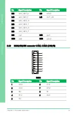
Page 31: ...4 8 POE LAN RJ 45 Connector CN11 Pin Signal Description Pin Signal Description R1A LAN2_MDI0_N L1A LAN2_LED_100 R2A LAN2_MDI0_P L2A LAN2_LED_1000 R3A LAN2_MDI1_N L3A AGND R4A LAN2_MDI1_P L4A OUT2_LED R5A LAN2_MDI2_N R6A LAN2_MDI2_P R7A LAN2_MDI2_N R8A LAN2_MDI3_P R9A CAP R11A OUT2 R10A GND R12A AGND R1B LAN1_MDI0_N L1B LAN1_LED_100 R2B LAN1_MDI0_P L2B LAN1_LED_1000 ...

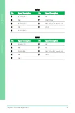
Page 32: ...1_N L3B AGND R4B LAN1_MDI1_P L4B OUT1_LED R5B LAN1_MDI2_N R6B LAN1_MDI2_P R7B LAN1_MDI3_N R8B LAN1_MDI3_P R9B CAP R11B OUT1 R10B GND R12B AGND 2 4 9 RS232 422 485 connector COM1 COM2 CN12 13 RS232 Pin Signal Description Pin Signal Description 1 DCD2 6 CTS2 2 DSR2 7 DTR2 3 RX2 8 RI1 4 RTS2 9 GND 5 TX2 1 2 3 4 5 6 7 8 9 ...

Page 33: ...2 Pin Signal Description Pin Signal Description 1 RS422_TX2 6 NC 2 NC 7 RS422_RX2 3 RS422_TX2 8 NC 5V 12V max 0 5A 4 NC 9 GND 5 RS422_RX2 RS485 Pin Signal Description Pin Signal Description 1 RS485_ D2 6 NC 2 NC 7 NC 3 RS485_D2 8 NC 5V 12V max 0 5A 4 NC 9 GND 5 NC ...

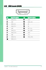
Page 34: ... PUC 2 4 10 HDMI Connector CN14 15 Pin Signal Description Pin Signal Description 1 HDMI_TX2 11 GND 2 GND 12 HDMI_CLK 3 HDMI_TX2 13 NC 4 HDMI_TX1 14 NC 5 GND 15 DDC_CLK 6 HDMI_TX1 16 DDC_DATA 7 HDMI_TX0 17 GND 8 GND 18 5V 9 HDMI_TX0 19 HDMI_HPD 10 HDMI_CLK ...

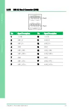
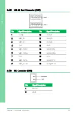
Page 35: ...2 4 11 USB 3 2 Gen 2 Connector CN16 Pin Signal Description Pin Signal Description 1 5VSB 10 5VSB 2 USB1_D 11 USB2_D 3 USB1_D 12 USB2_D 4 GND 13 GND 5 USB1_SSRX 14 USB2_SSRX 6 USB1_SSRX 15 USB2_SSRX 7 GND 16 GND 8 USB1_SSTX 17 USB2_SSTX 9 USB1_SSTX 18 USB2_SSTX ...

Page 36: ...N17 Pin Signal Description Pin Signal Description 1 5VSB 10 5VSB 2 USB3_D 11 USB4_D 3 USB3_D 12 USB4_D 4 GND 13 GND 5 USB3_SSRX 14 USB4_SSRX 6 USB3_SSRX 15 USB4_SSRX 7 GND 16 GND 8 USB3_SSTX 17 USB4_SSTX 9 USB3_SSTX 18 USB4_SSTX 2 4 13 RTC Connector CN18 Pin Signal Description 1 RTCVCC 2 GND ...

Page 37: ...n 1 VCC 2 VCC 3 USBD 4 USBD 5 USBD 6 USBD 7 GND 8 GND 9 GND 10 GND 2 4 15 Mini Card Connector CN20 Pin Signal Description Pin Signal Description 1 PCIE_WAKE 27 GND 2 3 3VSB 28 1 5V 3 NC 29 GND 4 GND 30 SMB_CLK 5 NC 31 PCIE_TX 6 1 5V 32 SMB_DATA 7 IN 33 PCIE_TX 8 UIM_PWR 34 GND 9 GND 35 GND 10 UIM_DATA 36 USB_D 11 PCIE_REF_CLK 37 GND ...

Page 38: ...IM_CLK 38 USB_D 13 PCIE_REF_CLK 39 3 3VSB 14 UIM_RST 40 GND 15 GND 41 3 3VSB 16 UIM_VPP 42 NC 17 NC 43 GND 18 GND 44 NC 19 NC 45 NC 20 W_DISABLE 46 NC 21 GND 47 NC 22 PCIE_RST 48 1 5V 23 PCIE_RX 49 NC 24 3 3VSB 50 GND 25 PCIE_RX 51 NC 26 GND 52 3 3VSB 2 4 16 DDR4 SO DIMM Slot DIMM1 DIMM2 Standard specification ...

Page 39: ... List of Jumpers POE Board Label Function JP1 OUT2 Select JP2 AGND2 Select JP3 AGND1 Select JP4 OUT1 Select 2 5 1 OUT2 Select JP1 OUT2_1236 Default OUT2_4578 2 5 2 AGND2 Select JP2 AGND2_1236 Default AGND2_4578 2 5 3 AGND1 Select JP3 AGND1_1236 Default AGND1_4578 ...

Page 40: ...Chapter 2 Hardware Information 27 EPIC Board EPIC CFS7 PUC 2 5 4 OUT1 Select JP4 OUT1_1236 Default OUT1_4578 ...

Page 41: ...12V DC IN CN2 LAN2 RJ 45 Port CN3 LAN1 RJ 45 Port CN4 FPC Cable Port Connect to EPIC CFS7 2 6 1 12V DC In CN1 Pin Pin Name Signal Type Signal Level 1 GND GND 2 GND GND 3 V_IN PWR 12V 4 V_IN PWR 12V 2 6 2 LAN RJ 45 Port CN2 CN3 Pin Pin Name Signal Type Signal Level 1 TRP1 DIFF 2 TRP1 DIFF 3 TRP2 DIFF 4 TRP3 DIFF ...

Page 42: ...ame Signal Type Signal Level 5 TRP3 DIFF 6 TRP2 DIFF 7 TRP4 DIFF 8 TRP4 DIFF 2 6 3 FPC Cable Port CN4 Pin Pin Name Signal Type Signal Level 1 V12S PWR 12V 2 V12S PWR 12V 3 V12S PWR 12V 4 V12S PWR 12V 5 V12S PWR 12V 6 GND GND 7 PCIE_9_TXP DIFF 8 PCIE_9_TXN DIFF 9 GND GND ...

Page 43: ... PCIE_10_TXN DIFF 15 GND GND 16 PCIE_11_TXP DIFF 17 PCIE_11_TXN DIFF 18 GND GND 19 PCIE_12_TXP DIFF 20 PCIE_12_TXN DIFF 21 GND GND 22 PCIE_9_RXN DIFF 23 PCIE_9_RXP DIFF 24 GND GND 25 PCIE_11_RXN DIFF 26 PCIE_11_RXP DIFF 27 GND GND 28 PCIE_12_RXN DIFF 29 PCIE_12_RXP DIFF 30 GND GND 31 PCIE_10_RXN DIFF 32 PCIE_10_RXP DIFF 33 GND GND 34 V3P3A DIFF 3 3V 35 BUF_PLT_RST I O 3 3V ...

Page 44: ...Chapter 2 Hardware Information 31 EPIC Board EPIC CFS7 PUC Pin Pin Name Signal Type Signal Level 36 SMB_CLK I O 3 3V 37 SMB_DATA I O 3 3V 38 V3P3S 3 3V 39 V3P3S 3 3V 40 V3P3S 3 3V ...

Page 45: ...ard Note There are no jumpers on DIO Board Label Function CN1 LPC Port CN2 Power In from EPIC CFS7 CN3 GPI Port CN4 GPO Port 2 7 1 LPC Port CN1 Pin Pin Name Signal Type Signal Level 1 LPC_AD0 I O 3 3V 2 LPC_AD1 I O 3 3V 3 LPC_AD2 I O 3 3V 4 LPC_AD3 I O 3 3V 5 V3P3S PWR 3 3V 6 LPC_FRAME IN ...

Page 46: ...n Name Signal Type Signal Level 7 BUF_PLT_RST IN 3 3V 8 GND GND 9 CLK_LPC_25M_DBG OUT 10 SMB_DATA_3P3 I O 3 3V 11 SMB_CLK_3P3 IN 3 3V 12 SMB_ALERT _3P I O 3 3V 2 7 2 Power In CN2 Pin Pin Name Signal Type Signal Level 1 V5S PWR 5V 2 V3P3S PWR 3 3V 3 GND GND 4 GND GND ...

Page 47: ...in Name Signal Type Signal Level 1 GPI0 IN 12V 24V 2 GPI1 IN 12V 24V 3 GPI2 IN 12V 24V 4 GPI3 IN 12V 24V 5 GPI4 IN 12V 24V 6 GPI5 IN 12V 24V 7 GPI6 IN 12V 24V 8 GPI7 IN 12V 24V 9 NC NC 10 PC_VDD PWR 12V 24V 11 GPI8 IN 12V 24V 12 GPI9 IN 12V 24V 13 GPI10 IN 12V 24V 14 GPI11 IN 12V 24V ...

Page 48: ...al Level 15 GPI12 IN 12V 24V 16 GPI13 IN 12V 24V 17 GPI14 IN 12V 24V 18 GPI15 IN 12V 24V 19 NC NC 20 PC_VDD PWR 12V 24V 2 7 4 GPO Port CN4 Pin Pin Name Signal Type Signal Level 1 GPO0 OUT 12V 24V 2 GPO1 OUT 12V 24V 3 GPO2 OUT 12V 24V 4 GPO3 OUT 12V 24V 5 GPO4 OUT 12V 24V 6 GPO5 OUT 12V 24V ...

Page 49: ...Signal Type Signal Level 7 GPO6 OUT 12V 24V 8 GPO7 OUT 12V 24V 9 NC NC 10 PC_GND GND 11 GPO8 OUT 12V 24V 12 GPO9 OUT 12V 24V 13 GPO10 OUT 12V 24V 14 GPO11 OUT 12V 24V 15 GPO12 OUT 12V 24V 16 GPO13 OUT 12V 24V 17 GPO14 OUT 12V 24V 18 GPO15 OUT 12V 24V 19 NC NC 20 PC_GND GND ...

Page 50: ...Chapter 2 Hardware Information 37 EPIC Board EPIC CFS7 PUC 2 8 Block Diagrams ...

Page 51: ...Chapter 2 Hardware Information 38 EPIC Board EPIC CFS7 PUC ...

Page 52: ...39 EPIC Board EPIC CFS7 PUC Chapter 3 Chapter 3 BIOS Setup ...

Page 53: ...red on the CMOS memory and BIOS NVRAM If the system configuration is not found or a system configuration data error is detected the system will load the optimized default and re boot with this default system configuration automatically There are four situations in which you will need to setup System Configuration 1 You are starting your system for the first time 2 You have changed the hardware att...

Page 54: ...mation when the power is turned off To enter setup power on the computer and press Del or ESC immediately The following are short descriptions of each submenu Main Date and time can be set here Press Tab to switch between date elements Advanced Enable Disable boot options for legacy network devices Chipset Host bridge parameters Security The setup administrator password can be set here Boot Enable...

Page 55: ...Chapter 3 BIOS Setup 42 EPIC Board EPIC CFS7 PUC 3 3 Setup Submenu Main ...

Page 56: ...Chapter 3 BIOS Setup 43 EPIC Board EPIC CFS7 PUC 3 4 Setup Submenu Advanced ...

Page 57: ...ault When enabled a VMM can utilize the additional hardware capabilities provided by Vanderpool Technology C States Disabled Enabled Optimal Default Failsafe Default Enable Disable C States Intel R SpeedStep tm Disabled Enabled Optimal Default Failsafe Default Allows more than two frequency ranges to be supported Turbo Mode Disabled Enabled Optimal Default Failsafe Default Enable Disable processor...

Page 58: ...ons Summary SATA Controller s Disabled Enabled Optimal Default Failsafe Default Enable Disable SATA Device Port 0 Disabled Optimal Default Failsafe Default Enabled Enable or Disable SATA Port mSATA port Disabled Enabled Optimal Default Failsafe Default Enable or Disable SATA Port ...

Page 59: ...Chapter 3 BIOS Setup 46 EPIC Board EPIC CFS7 PUC 3 4 3 Hardware Monitor ...

Page 60: ...e fans Linear fan application circuit to control 3 wire fan speed by fan s power terminal Output PWM mode open drain to control Intel 4 wire fans Fan Mode Auto RPM Mode Auto Duty Cycle Mode Optimal Default Failsafe Default Smart Fan Mode Select Temperature Source CPU CPU external Optimal Default Failsafe Default System Select the monitored temperature source for this fan Duty Cycle Auto fan speed ...

Page 61: ...Chapter 3 BIOS Setup 48 EPIC Board EPIC CFS7 PUC Auto RPM Mode Options Summary RPM Percentage Auto fan speed control Fan speed will follow different temperature by different RPM 1 100 Temperature ...

Page 62: ...er 3 BIOS Setup 49 EPIC Board EPIC CFS7 PUC Manual Duty Mode Options Summary Manual Duty Mode 60 Optimal Default Failsafe Default Manual mode fan control user can write expected duty cycle PWM fan type 1 100 ...

Page 63: ...Chapter 3 BIOS Setup 50 EPIC Board EPIC CFS7 PUC 3 4 4 SIO Configuration ...

Page 64: ...ilsafe Default Enable or Disable this Logical Device Possible Use Automatic Settings Optimal Default Failsafe Default IO 3F8h IRQ 4 IO 2F8h IRQ 3 Allows user to change Device s Resource settings New settings will be reflected on This Setup Page after System restarts Mode RS232 Optimal Default Failsafe Default RS422 RS485 UART RS232 422 485 selection ...

Page 65: ...ilsafe Default Enable or Disable this Logical Device Possible Use Automatic Settings Optimal Default Failsafe Default IO 2F8h IRQ 3 IO 3F8h IRQ 4 Allows user to change Device s Resource settings New settings will be reflected on This Setup Page after System restarts Mode RS232 Optimal Default Failsafe Default RS422 RS485 UART RS232 422 485 selection ...

Page 66: ...ptimal Default Failsafe Default Always On Always Off IO Restore AC power Loss RTC wake system from S5 Disable Optimal Default Failsafe Default Fixed Time Dynamic Time Fixed Time System will wake on the hr min sec specified n Dynamic Time System will wake on the current time Increase minute s Wake on LAN Enable Enabled Optimal Default Failsafe Default Disabled Enable Disable integrated LAN to wake ...

Page 67: ...54 EPIC Board EPIC CFS7 PUC 3 4 6 Digital IO Port Configuration Options Summary DIO Port Output Input Set DIO as Input or Output Output Level High Optimal Default Failsafe Default Low Set output level when DIO pin is output ...

Page 68: ...Chapter 3 BIOS Setup 55 EPIC Board EPIC CFS7 PUC 3 5 Setup Submenu Chipset ...

Page 69: ...Chapter 3 BIOS Setup 56 EPIC Board EPIC CFS7 PUC 3 5 1 System Agent SA Configuration ...

Page 70: ...o Disabled Enabled Optimal Default Failsafe Default Control Detection of the HD Audio device Disabled HDA will be unconditionally disabled Enabled HDA will be unconditionally enabled MiniCard Slot Function SATA Optimal Default Failsafe Default PCIe Select function enabled for Half MiniCard CN20 slot ...

Page 71: ...he user enters the Setup utility A User Password does not provide access to many of the features in the Setup utility Select the password you wish to set and press Enter In the dialog box enter your password must be between 3 and 20 letters or numbers Press Enter and retype your password to confirm Press Enter again to set the password Removing the Password Select the password you want to remove a...

Page 72: ... in User mode The mode change requires platform reset Secure Boot Mode Custom Optimal Default Failsafe Default Standard Secure Boot mode options Standard or Custom In Custom mode Secure Boot Policy variables can be configured by a physically present user without full authentication Restore Factory Keys Force System to User Mode Install factory default Secure Boot key databases Reset To Setup Mode ...

Page 73: ...Force System to User Mode Install factory default Secure Boot key databases Reset To Setup Mode Delete all Secure Boot key databases from NVRAM Export Secure Boot variables Copy NVRAM content of Secure Boot variables to files in a root folder on a file system device Enroll Efi Image Allow the image to run in Secure Boot mode Enroll SHA256 Hash certificate of a PE image into Authorized Signature Da...

Page 74: ...ed Signatures Details Export Update Append Delete Forbidden Signatures Details Export Update Append Delete Authorized TimeStamps Update Append OsRecovery Signatures Update Append Enroll Factory Defaults or load certificates from a file 1 Public Key Certificate a EFI_SIGNATURE_LIST b EFI_CERT_X509 DER c EFI_CERT_RSA2048 bin d EFI_CERT_SHAXXX 2 Authenticated UEFI Variable 3 EFI PE COFF Image SHA256 ...

Page 75: ...7 Setup Submenu Boot Options Summary Quiet Boot Disabled Enabled Optimal Default Failsafe Default Enable or disable showing boot logo Lunch PXE ROM Disabled Optimal Default Failsafe Default Enabled Controls the execution of UEFI and Legacy Network OpROM ...

Page 76: ...Chapter 3 BIOS Setup 63 EPIC Board EPIC CFS7 PUC 3 7 1 BBS Priorities ...

Page 77: ...Chapter 3 BIOS Setup 64 EPIC Board EPIC CFS7 PUC 3 8 Setup Submenu Save Exit ...

Page 78: ...65 EPIC Board EPIC CFS7 PUC Chapter 4 Chapter 4 Driver Installation ...

Page 79: ...f your operating system OS is compatible with the drivers AAEON provides for the EPIC CFS7 PUC Some drivers are limited in their compatibility and will only work with certain operating systems If you have any questions contact your AAEON sales representative for assistance OS Compatibility Table Driver Windows 10 64 bit Linux Step 1 Chipset Yes No Step 2 Graphics Yes No Step 3 Network Yes No Step ...

Page 80: ...nstructions 4 Drivers will be installed automatically Step 3 Install Network Drivers 1 Open the Step 3 Network folder 2 Open the ProWinx64 exe file in the folder 3 Follow the instructions 4 Drivers will be installed automatically Step 4 Install ME Drivers 1 Open the Step 4 ME folder 2 Open the SetupME exe file in the folder 3 Follow the instructions 4 Drivers will be installed automatically ...

Page 81: ...EPIC Board EPIC CFS7 PUC Appendix A Appendix A I O Information ...

Page 82: ...Appendix A I O Information 69 EPIC Board EPIC CFS7 PUC A 1 I O Address Map ...

Page 83: ...Appendix A I O Information 70 EPIC Board EPIC CFS7 PUC ...

Page 84: ...Appendix A I O Information 71 EPIC Board EPIC CFS7 PUC ...

Page 85: ...Appendix A I O Information 72 EPIC Board EPIC CFS7 PUC A 2 Memory Address Map ...

Page 86: ...Appendix A I O Information 73 EPIC Board EPIC CFS7 PUC A 3 IRQ Mapping Chart ...

Page 87: ...Appendix A I O Information 74 EPIC Board EPIC CFS7 PUC ...

Page 88: ...Pico ITX Board EPIC CFS7 PUC Appendix B Appendix B Watchdog Timer Programming ...

Page 89: ...1 Enable Disable time out output via WDTRST 0 Disable 1 Enable Pulse Width 0x05 0 1 01 Width of Pulse signal 00 1ms do not use 01 25ms 10 125ms 11 5s Pulse width is must longer then 16ms Signal Polarity 0x05 2 0 0 low active 1 high active Must set this bit to 0 Counting Unit 0x05 3 0 Select time unit 0 second 1 minute Output Signal Type 0x05 4 1 0 Level 1 Pulse Must set this bit to 1 Watchdog Time...

Page 90: ...ster define PSWidthBit 0x00 WDTRST Pulse width Bit0 1 define PSWidthVal 0x01 25ms for WDTRST pulse define PolarityBit 0x02 WDTRST Signal polarity Bit2 define PolarityVal 0x00 Low active for WDTRST define UnitBit 0x03 Unit for timer Bit3 define ModeBit 0x04 WDTRST mode Bit4 define ModeVal 0x01 0 level 1 pulse define EnableBit 0x05 WDT timer enable Bit5 define EnableVal 0x01 1 enable define StatusBi...

Page 91: ...onWDTEnable VOID AaeonWDTEnable WDTEnableDisable 1 Procedure AaeonWDTConfig VOID AaeonWDTConfig byte Counter BOOLEAN Unit Disable WDT counting WDTEnableDisable 0 Clear Watchdog Timeout Status WDTClearTimeoutStatus WDT relative parameter setting WDTParameterSetting Timer Unit VOID WDTEnableDisable byte Value If Value 1 WDTSetBit TimerReg EnableBit 1 else WDTSetBit TimerReg EnableBit 0 VOID WDTParam...

Page 92: ...h is 25ms WDTSetBit TimerReg PSWidthBit PSWidthVal Watchdog WDTRST Enable WDTSetBit DevReg WDTRstBit WDTRstVal VOID WDTClearTimeoutStatus WDTSetBit TimerReg StatusBit 1 VOID WDTWriteByte byte Register byte Value IOWriteByte WDTAddr Register Value byte WDTReadByte byte Register return IOReadByte WDTAddr Register VOID WDTSetBit byte Register byte Bit byte Val byte TmpValue TmpValue WDTReadByte Regis...

Reviews: