background image


Chapter 2 – Hardware Information 


30


Net
work 

Ap

plian
ce


FW

S-

78

31 


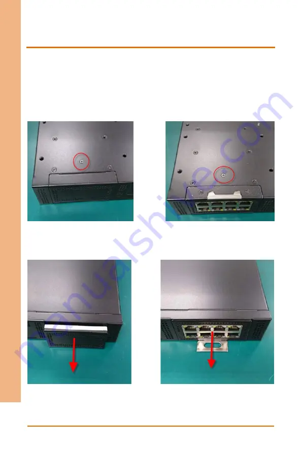
2.8  Installing NIM 


This section details the steps of how to install NIM modules for the FWS-7831. This 

applies for new installation, or removal/replacement of modules. 


1.


Remove the highlighted screw on the chassis bottom. 


2.


Remove the null module cover or existing module. 


Summary of Contents for AAEON FWS-7831

Page 1: ...Last Updated June 11 2019 FWS 7831 Network Appliance User s Manual 1st Ed ...

Page 2: ...in this manual is intended to be accurate and reliable However the original manufacturer assumes no responsibility for its use or for any infringements upon the rights of third parties that may result from its use The material in this document is for product information only and is subject to change without notice While reasonable efforts have been made in the preparation of this document to assur...

Page 3: ...rademark of Microsoft Corp Intel Pentium Celeron and Xeon are registered trademarks of Intel Corporation Core Atom are trademarks of Intel Corporation ITE is a trademark of Integrated Technology Express Inc IBM PC AT PS 2 and VGA are trademarks of International Business Machines Corporation All other product names or trademarks are properties of their respective owners ...

Page 4: ...1 Packing List Before setting up your product please make sure the following items have been shipped Item Quantity FWS 7831 1 If any of these items are missing or damaged please contact your distributor or sales representative immediately ...

Page 5: ...descriptions and explanations on the product s hardware and software features if any its specifications dimensions jumper connector settings definitions and driver installation instructions if any to facilitate users in setting up their product Users may refer to the product page at AAEON com for the latest version of this document ...

Page 6: ...system s hardware 6 No connections should be made when the system is powered as a sudden rush of power may damage sensitive electronic components 7 If the device is not to be used for a long time disconnect it from the power supply to avoid damage by transient over voltage 8 Always disconnect this device from any AC supply before cleaning 9 While cleaning use a damp cloth instead of liquid or spra...

Page 7: ...s 18 If any of the following situations arises please the contact our service personnel i Damaged power cord or plug ii Liquid intrusion to the device iii Exposure to moisture iv Device is not working as expected or in a manner as described in this manual v The device is dropped or damaged vi Any obvious signs of damage displayed on the device 19 DO NOT LEAVE THIS DEVICE IN AN UNCONTROLLED ENVIRON...

Page 8: ...osion if the battery is incorrectly replaced Replace only with the same or equivalent type recommended by the manufacturer Dispose of used batteries according to the manufacturer s instructions and your local government s recycling or disposal directives Attention Il y a un risque d explosion si la batterie est remplacée de façon incorrecte Ne la remplacer qu avec le même modèle ou équivalent reco...

Page 9: ...Preface IX Network Appliance FWS 7831 China RoHS Requirements CN ...

Page 10: ...Preface X Network Appliance FWS 7831 China RoHS Requirement EN ...

Page 11: ...ower Connector CN4 CN5 13 2 4 2 Digital I O CN17 13 2 4 3 LCM Connector CN18 14 2 4 4 Key PAD Connector CN19 14 2 4 5 COM Port COM2 15 2 4 6 Front Panel Pin Header FP1 15 2 4 7 USB 3 0 Port USB1 16 2 5 3 5 Hard Drive Installation 17 2 6 2 5 Hard Drive Installation 20 2 7 CPU and Heat Sink Installation 25 2 8 Installing NIM 30 Chapter 3 AMI BIOS Setup 32 3 1 System Test and Initialization 33 3 2 AM...

Page 12: ...Redirection 50 3 4 7 2 Legacy Console Redirection Settings 52 3 4 8 Advanced Power Management 53 3 4 9 Advanced Digital IO Port Configuration 54 3 4 10 Advanced LAN Bypass Configuration 55 3 4 11 Advanced Network Stack Configuration 56 3 5 Setup submenu Chipset 57 3 5 1 Chipset System Agent SA Configuration 58 3 6 Setup submenu Security 59 3 6 1 Security Secure Boot 60 3 6 1 1 Secure Boot Key Mana...

Page 13: ... Appendix C Standard LAN Bypass Platform Setting 79 C 1 Status LED 80 C 1 1 Status LED Configuration 80 C 1 2 Sample Code 81 C 2 LAN Bypass 83 C 2 1 LAN Bypass Configuration 83 C 2 2 Sample Code 85 C 3 Software Reset Button General Propose Input 87 C 3 1 Software Reset Button Configuration 87 C 3 2 Sample Code 88 ...

Page 14: ...Network Appliance FWS 7831 Chapter 1 Chapter 1 Product Specifications ...

Page 15: ...n H310 Chipset Chipset Intel C246 H310 System Memory 2x DDR4 SO DIMM ECC Up to 32GB DDR4 1600 1866 2133 SO DIMM ECC Up to 32GB 260 pin DIMM x 2 Network Ethernet Intel i211 Gigabit Ethernet x 8 or Intel i211 Gigabit Ethernet x 6 with SFP Ethernet ports x2 C246 Intel i211 Gigabit Ethernet x 6 H310 Bypass 2 Pairs NIM Slot 1 Display Graphic Controller Intel UHD Graphics 630 Connector HDMI x1 Optional ...

Page 16: ...rnal Interface PCIe slot NIM Slot x 1 Mini PCIe slot Mini Card x 1 PCIe x1 mSATA Keyboard and Mouse N A Universal Serial Bus USB 3 0 x 2 Miscellaneous RTC Internal RTC Watchdog Timer 1 255 steps by software programmable Software Button GPIO Programmable push button x 1 TPM TPM v2 0 9665 optional TPM v1 2 9660 optional GPIO 4 bits input 4bits output FAN 2 MTBF Hours TBD Color Black ...

Page 17: ...ative humidity non condensing Storage Humidity 10 80 40 C non condensing Vibration 0 5 g rms 5 500Hz operation 2 5 Hard Disk Drive 1 5 g rms 5 500Hz non operation Shock TBD Chassis Dimension W x D x H 16 93 x 7 87 x1 73 430mm x 200mm x 44mm I O Interface Front Panel Power LED x 1 Status LED x 1 HDD Active LED x 1 USB 3 0 Ports x 2 RJ 45 Console x 1 Rear Panel AC Power Input x 1 Power Switch x 1 Re...

Page 18: ...Network Appliance FWS 7831 Chapter 2 Chapter 2 Hardware Information ...

Page 19: ...Chapter 2 Hardware Information 6 Network Appliance FWS 7831 2 1 Dimensions System ...

Page 20: ...Chapter 2 Hardware Information 7 Network Appliance FWS 7831 Component Side ...

Page 21: ...Chapter 2 Hardware Information 8 Network Appliance FWS 7831 Solder Side ...

Page 22: ...Chapter 2 Hardware Information 9 Network Appliance FWS 7831 2 2 Jumpers and Connectors Component Side ...

Page 23: ...Chapter 2 Hardware Information 10 Network Appliance FWS 7831 Solder Side ...

Page 24: ...gured with a number of jumpers which can be configured for your application This section details those jumpers and their settings Label Function JP1 RTC Reset JP2 Auto Power Button 2 3 1 RTC Reset JP1 Normal Default 1 2 Clear CMOS 2 3 2 3 2 Auto Power Button JP2 Don t use Auto PWRBTN Default 1 2 Use Auto PWRBTN 2 3 ...

Page 25: ...connecting with external modules This section details those connectors and settings Label Function CN4 CN5 HDD Power Connector CN9 mSATA SOCKET CN17 Digital I O CN18 LCM Connector CN19 Key PAD Connector CN20 SYS_FAN1 CN21 SYS_FAN2 CN22 24 Pin ATX Power Connector CN23 8 Pin 12V Power Connector CN25 HDMI Connector COM2 COM Port FP1 Front Panel Pin Header SATA1 SATA2 SATA Port Connector USB1 USB3 0 P...

Page 26: ...CN5 Pin Signal Signal Type 1 12V PWR 2 GND GND 3 GND GND 4 5V PWR 2 4 2 Digital I O CN17 Pin Signal Signal Type 1 DIO0 Input Output 2 DIO1 Input Output 3 DIO2 Input Output 4 DIO3 Input Output 5 DIO4 Input Output 6 DIO5 Input Output 7 DIO6 Input Output 8 DIO7 Input Output 9 3 3V PWR 10 GND GND ...

Page 27: ... 5 INIT Output 6 AFD Output 7 DATA0 Input Output 8 DATA1 Input Output 9 DATA2 Input Output 10 DATA3 Input Output 11 DATA4 Input Output 12 DATA5 Input Output 13 DATA6 Input Output 14 DATA7 Input Output 15 5V PWR 16 LCD Output 2 4 4 Key PAD Connector CN19 Pin Signal Signal Type 1 KEY PAD Down Input 2 KEY PAD Up Input 3 KEY PAD Right Input 4 KEY PAD Left Input ...

Page 28: ...Input 2 RXD Input 3 TXD Output 4 DTR Output 5 GND GND 6 DSR Input 7 RTS Output 8 CTS Input 9 RI Input 10 N C 2 4 6 Front Panel Pin Header FP1 Pin Signal Signal Type 1 Power On Button Input 2 Power On Button GND 3 Reset Switch Input 4 Reset Switch GND 5 Power LED POWER 6 Power LED GND 7 HDD LED Output 8 HDD LED Output ...

Page 29: ...nal Type 1 5V_USB PWR 2 USB3_RX1_DN DIFF 3 USB3_RX1_DP DIFF 4 GND GND 5 USB3_TX1_DN DIFF 6 USB3_TX1_DP DIFF 7 GND GND 8 USBP_0N DIFF 9 USBP_0P DIFF 10 NC 11 USBP_1P DIFF 12 USBP_1N DIFF 13 GND GND 14 USB3_TX2_DP DIFF 15 USB3_TX2_DN DIFF 16 GND GND 17 USB3_RX2_DP DIFF 18 USB3_RX2_DN DIFF 19 5V_USB PWR ...

Page 30: ...WS 7831 2 5 3 5 Hard Drive Installation This section details the steps of how to install a 3 5 hard drive for the FWS 7831 1 Remove the screws securing the top cover then remove the cover 2 Install the bracket cushions on the hard drive brackets as shown ...

Page 31: ...Chapter 2 Hardware Information 18 Network Appliance FWS 7831 3 Install brackets onto hard drive with screws ...

Page 32: ...ter 2 Hardware Information 19 Network Appliance FWS 7831 4 Fasten the assembled hard drive and brackets to the chassis with screws 5 Connect the SATA cable and power cable to the hard drive and system board ...

Page 33: ...tion This section details the steps of how to install a 2 5 hard drive for the FWS 7831 This section includes steps for installing one or two 2 5 hard drives 1 Remove the screws securing the top cover then remove the cover 2 Install the bracket cushions on the hard drive brackets as shown ...

Page 34: ...work Appliance FWS 7831 3 Install brackets onto hard drive with screws Repeat Steps 2 3 with the second set of brackets if you are installing two hard drives 4 Attach SATA and power cables to system board as shown for the first hard drive ...

Page 35: ...Attach SATA and power cables to system board as shown for the second hard drive skip this step if only installing one hard drive 6 Place first hard drive assembly onto installation brackets as shown Note Make sure that SATA and power cables are under the hard drive ...

Page 36: ...tion 23 Network Appliance FWS 7831 7 Connect SATA and power cable to first hard drive as shown 8 Place the second hard drive onto installation brackets as shown Note Make sure that SATA and power cables are under the hard drive ...

Page 37: ...Chapter 2 Hardware Information 24 Network Appliance FWS 7831 9 Connect SATA and power cable to the second hard drive as shown ...

Page 38: ... FWS 7831 2 7 CPU and Heat Sink Installation This section details the steps of how to install the CPU and heat sink for the FWS 7831 1 Remove the screws securing the top cover then remove the cover 2 Remove the highlighted screw then remove the fan duct ...

Page 39: ...Chapter 2 Hardware Information 26 Network Appliance FWS 7831 3 Open the CPU bracket ...

Page 40: ...FWS 7831 4 Remove the pin cover and place the CPU into the socket Use the notches to ensure proper alignment Note The CPU should fit into the socket easily DO NOT force the CPU into the socket Pushing on the CPU can cause damage to the CPU pins or socket ...

Page 41: ...lock the bracket pole into position Note Please ensure you have applied thermal paste according to CPU manufacturer s guidelines before installing the heat sink 6 Place the heatsink onto the CPU and fasten the heatsink screws Make sure the heatsink is aligned with the airflow of the fan ...

Page 42: ...Chapter 2 Hardware Information 29 Network Appliance FWS 7831 7 Replace the fan cover and secure with the fastening screw ...

Page 43: ...8 Installing NIM This section details the steps of how to install NIM modules for the FWS 7831 This applies for new installation or removal replacement of modules 1 Remove the highlighted screw on the chassis bottom 2 Remove the null module cover or existing module ...

Page 44: ...Chapter 2 Hardware Information 31 Network Appliance FWS 7831 3 Insert the new module or null module cover firmly and secure with the screw ...

Page 45: ...Network Appliance FWS 7831 Chapter 3 Chapter 3 AMI BIOS Setup ...

Page 46: ...rification routines check the current system configuration against the values stored in the CMOS memory If they do not match an error message will be output and the BIOS setup program will need to be run to set the configuration information in memory There are three situations in which the CMOS settings will need to be set or changed Starting the system for the first time The system hardware has b...

Page 47: ... when the power is turned off To enter BIOS Setup press Del or F2 immediately while your computer is powering up The function for each interface can be found below Main Date and time can be set here Press Tab to switch between date elements Advanced Enable Disable boot option for legacy network devices Chipset Host bridge parameters Security The setup administrator password can be set here Boot En...

Page 48: ...Chapter 3 AMI BIOS Setup 35 Network Appliance FWS 7831 3 3 Setup Submenu Main ...

Page 49: ...Chapter 3 AMI BIOS Setup 36 Network Appliance FWS 7831 3 4 Setup Submenu Advanced ...

Page 50: ...ge Hyper Threading Disabled Enabled Optimal Default Failsafe Default Enabled for Windows XP and Linux OS optimized for Hyper Threading Technology and Disabled for other OS OS not optimized for Hyper Threading Technology Intel Speed Shift Technology Disable Optimal Default Failsafe Default Enable Enable Disable Intel Speed Shift Technology support Enabling will expose the CPPC v2 interface to allow...

Page 51: ...Chapter 3 AMI BIOS Setup 38 Network Appliance FWS 7831 3 4 2 Advanced PCH FW Configuration ...

Page 52: ...Firmware Update Configuration Options Summary Me FW Image Re Flash Disabled Optimal Default Failsafe Default Enabled Enable Disable Me FW Image Re Flash function Local FW Update Disabled Enabled Optimal Default Failsafe Default Options for Local FW Update function ...

Page 53: ...le Disable Security Device Note Your Computer will reboot during restart in order to change State of the Device Pending operation None Optimal Default Failsafe Default TPM Clear Schedule an Operation for the Security Device Note Your Computer will reboot during restart in order to change State of Security Device Device Select TPM 1 2 TPM 2 0 Auto Optimal Default Failsafe Default TPM 1 2 will restr...

Page 54: ...s Enabled Optimal Default Failsafe Default Disabled Enable Disable SATA Device SATA Mode Selection AHCI Optimal Default Failsafe Default Intel RST Premium With Intel Optane System Acceleration Determines how SATA controller s operate Hot Plug Disabled Optimal Default Failsafe Default Enabled Designates this port as Hot Pluggable ...

Page 55: ...Chapter 3 AMI BIOS Setup 42 Network Appliance FWS 7831 3 4 5 Advanced Hardware Monitor ...

Page 56: ...rdance with user settings Disabled FAN always operates at full speed FAN Control Mode Manual Mode Automatic Mode Optimal Default Failsafe Default Manual Mode Depends on PWM Duty Automatic Mode FAN Speed depends on CPU Temperature Spin PWM 80 Optimal Default Failsafe Default The PWM Duty of FAN Spin Range 0 255 Temperature Source System Temperature CPU Temperature DTS Optimal Default Failsafe Defau...

Page 57: ...en if the PWM value is 0 Start Control Temperature 60 Optimal Default Failsafe Default Temperature Value for FAN Start Full Speed Temperature 95 Optimal Default Failsafe Default Temperature Value for FAN Full Speed PWM Slope 1 Optimal Default Failsafe Default Slope PWM value Degree C for FAN Speed Control Range 1 15 PWM Duty 200 Optimal Default Failsafe Default Manual Mode PWM Duty value Range 0 2...

Page 58: ...Chapter 3 AMI BIOS Setup 45 Network Appliance FWS 7831 3 4 6 Advanced SIO Configuration ...

Page 59: ...Chapter 3 AMI BIOS Setup 46 Network Appliance FWS 7831 3 4 6 1 Serial Port Configuration ...

Page 60: ...abled Enabled Optimal Default Failsafe Default Enable Disable this Logical Device Possible Use Automatic Settings Optimal Default Failsafe Default IO 3F8 IRQ 4 IO 2F8 IRQ 3 Allow user to change Device s Resource settings New settings will be reflected on This Setup Page after System restarts ...

Page 61: ...efault IO 378 IRQ 5 IO 378 IRQ 5 6 7 9 10 11 12 IO 278 IRQ 5 6 7 9 10 11 12 IO 3BC IRQ 5 6 7 9 10 11 12 Allow user to change Device s Resource settings New settings will be reflected on This Setup Page after System restarts Mode Standard Parallel Port mode SPP Optimal Default Failsafe Default EPP Mode ECP Mode EPP mode ECP mode Change Parallel Port mode Some of the Modes required a DMA resource Af...

Page 62: ... Summary COM0 Console Redirection Disabled Enabled Optimal Default Failsafe Default Enable or Disable Console Redirection Serial Port for Out of Band Management Windows Emergency Management Services EMS Console Redirection Disabled Optimal Default Failsafe Default Enabled Enable or Disable Console Redirection ...

Page 63: ...ion ANSI Extended ASCII char set VT100 ASCII char set VT100 Extends VT100 to support color function keys etc VT UTF8 Uses UTF8 encoding to map Unicode chars onto 1 or more bytes Bits per second 9600 19200 38400 57600 115200 Optimal Default Failsafe Default Selects serial port transmission speed The speed must be matched on the other side Long or noisy lines may require lower speeds ...

Page 64: ...s may require more than 1 stop bit Flow control None Optimal Default Failsafe Default Hardware RTS CTS Flow control can prevent data loss from buffer overflow When sending data if the receiving buffers are full a stop signal can be sent to stop the data flow Once the buffers are empty a start signal can be sent to re start the flow Hardware flow control uses two wires to send start stop signals VT...

Page 65: ...ages Resolution 80x24 Optimal Default Failsafe Default 80x25 On Legacy OS the Number of Rows and Columns supported redirection Redirection After POST Always Enable Optimal Default Failsafe Default BootLoader When BootLoader is selected then Legacy Console Redirection is disabled before booting to legacy OS When Always Enable is selected then Legacy Console Redirection is enabled for legacy OS Defa...

Page 66: ...t power supply mode Restore AC Power Loss Last State Optimal Default Failsafe Default Always On Always Off Select power state when power is re applied after a power failure RTC wake system from S5 Disabled Optimal Default Failsafe Default Enabled Fixed Time System will wake on the hr min sec Specified Dynamic Time System will wake on the current time Increase minutes s ...

Page 67: ...figuration Options Summary DIO Port1 4 Output Optimal Default Failsafe Default Input Set DIO as Input or Output Output Level High Optimal Default Failsafe Default Low Set output level when DIO pin is output DIO Port5 8 Output Input Optimal Default Failsafe Default Set DIO as Input or Output ...

Page 68: ...D FAST BLINK LAN Bypass Status LED Mode for Power on ByPass PassTru Optimal Default Failsafe Default Configure LAN kit behavior when system in power on state Bypass Pass Through Mode for Power off ByPass PassTru Optimal Default Failsafe Default Configure LAN kit behavior when system in power off state Bypass Pass Through WDT Configuration System Reset Optimal Default Failsafe Default Force ByPass ...

Page 69: ...sabled IPv4 PXE boot support will not be available Ipv4 HTTP Support Disabled Optimal Default Failsafe Default Enabled Enable Disable IPv4 HTTP boot support If disabled IPv4 HTTP boot support will not be available PXE boot wait time 0 Optimal Default Failsafe Default Wait time in seconds to press ESC key to abort the PXE boot Use either or numeric keys to set the value Media detect count 1 Optimal...

Page 70: ...Chapter 3 AMI BIOS Setup 57 Network Appliance FWS 7831 3 5 Setup submenu Chipset ...

Page 71: ...gent SA Configuration Options Summary VT d Disabled Enabled Optimal Default Failsafe Default VT d capability Primary Display Auto Optimal Default Failsafe Default IGFX PEG PCI Select which of IGFX PEG PCI Graphics device should be Primary Display Or select SG for Switchable Gfx ...

Page 72: ...n the user enters the Setup utility A User Password does not provide access to many of the features in the Setup utility Select the password you wish to set and press Enter In the dialog box enter your password must be between 3 and 20 letters or numbers Press Enter and retype your password to confirm Press Enter again to set the password Removing the Password Select the password you want to remov...

Page 73: ...e mode change requires platform reset Secure Boot Mode Standard Custom Optimal Default Failsafe Default In Custom mode Secure Boot Policy variables can be configured by a physically present user without full authentication Restore Factory Keys No Select Yes to restore factory default keys Yes Force System to User Mode Install factory default Secure Boot key databases Reset To Setup Mode No Select ...

Page 74: ...he System is in Setup mode Restore Factory Keys No Press Yes to restore factory default keys Yes Force System to User Mode Install factory default Secure Boot key databases Reset To Setup Mode No Press Yes to reset to setup mode Yes Delete all Secure Boot key databases from NVRAM Export Secure Boot variables Select a File system to export Secure Boot variables Copy NVRAM content of Secure Boot var...

Page 75: ...llow the image to run in Secure Boot mode Enroll SHA256 Hash certificate of a PE image into Authorized Signature Database db Remove UEFI CA from DB Device Guard ready system must not list Microsoft UEFI CA Certificate in Authorized Signature database db Restore DB defaults Press Yes to restore DB variable to factory defaults Restore DB variable to factory defaults ...

Page 76: ...option CSM Support Disabled Optimal Default Failsafe Default Enabled Enable Disable CSM Support Launch PXE ROM Do not launch Optimal Default Failsafe Default UEFI Legacy Controls the execution of UEFI and Legacy Network OpROM Note Network Stack should be enabled if select UEFI PXE boot Boot mode select Legacy UEFI Optimal Default Failsafe Default DUAL Select boot mode LEGACY UEFI ...

Page 77: ...Chapter 3 AMI BIOS Setup 64 Network Appliance FWS 7831 3 8 Setup submenu Save Exit ...

Page 78: ...Network Appliance FWS 7831 Chapter 4 Chapter 4 Drivers Installation ...

Page 79: ...he AAEON website by following this link https www aaeon com en p rackmount network appliance fws 7831 Download the driver s you need and follow the steps below to install them Step 1 LAN Drivers 1 Open the Step 1 LAN folder 2 Extract the archived file igb 5 3 5 22 tar gz 3 Extract the archived file igb 5 3 5 22 tar 4 Open igb 5 3 5 22 5 Follow instructions in README ...

Page 80: ...Network Appliance FWS 7831 Appendix A Appendix A Watchdog Timer Programming ...

Page 81: ...nP Mode Data Register 0x2F or 0x4F Table 2 Watchdog relative register table LDN Register BitNum Value Note Timer Counter 0x07 Note3 0x73 Note4 Note24 Time of watchdog timer 0 255 This register is byte access Counting Unit 0x07 Note5 0x72 Note6 7 Note7 1 Note8 Select time unit 1 second 0 minute Watchdog Enable KRST 0x07 Note9 0x72 Note10 6 Note11 1 Note12 0 Disable 1 Enable Timeout Status 0x07 Note...

Page 82: ... This parameter is represented from Note24 define byte UnitLDN This parameter is represented from Note5 define byte UnitReg This parameter is represented from Note6 define byte UnitBit This parameter is represented from Note7 define byte UnitVal This parameter is represented from Note8 define byte EnableLDN This parameter is represented from Note9 define byte EnableReg This parameter is represente...

Page 83: ...twork Appliance FWS 7831 VOID Main Procedure AaeonWDTConfig byte Timer Time of WDT timer 0x00 0xFF boolean Unit Select time unit 0 second 1 minute AaeonWDTConfig Procedure AaeonWDTEnable This procudure will enable the WDT counting AaeonWDTEnable ...

Page 84: ...nableReg EnableBit 0 Clear Watchdog Timeout Status WDTClearTimeoutStatus WDT relative parameter setting WDTParameterSetting VOID WDTEnableDisable byte LDN byte Register byte BitNum byte Value SIOBitSet LDN Register BitNum Value VOID WDTParameterSetting Watchdog Timer counter setting SIOByteSet TimerLDN TimerReg TimerVal WDT counting unit setting SIOBitSet UnitLDN UnitReg UnitBit UnitVal VOID WDTCl...

Page 85: ...x 0x01 IOWriteByte SIOIndex 0x55 IOWriteByte SIOIndex 0x55 Break Case 0x4E IOWriteByte SIOIndex 0x87 IOWriteByte SIOIndex 0x01 IOWriteByte SIOIndex 0x55 IOWriteByte SIOIndex 0xAA Break VOID SIOExitMBPnPMode IOWriteByte SIOIndex 0x02 IOWriteByte SIOData 0x02 VOID SIOSelectLDN byte LDN IOWriteByte SIOIndex 0x07 SIO LDN Register Offset 0x07 IOWriteByte SIOData LDN ...

Page 86: ...e SIOEnterMBPnPMode SIOSelectLDN byte LDN IOWriteByte SIOIndex Register TmpValue IOReadByte SIOData TmpValue 1 BitNum TmpValue Value BitNum IOWriteByte SIOData TmpValue SIOExitMBPnPMode VOID SIOByteSet byte LDN byte Register byte Value SIOEnterMBPnPMode SIOSelectLDN LDN IOWriteByte SIOIndex Register IOWriteByte SIOData Value SIOExitMBPnPMode ...

Page 87: ...Network Appliance FWS 7831 Appendix B Appendix B I O Information ...

Page 88: ...Appendix B I O Information 75 Network Appliance FWS 7831 B 1 I O Address Map ...

Page 89: ...Appendix B I O Information 76 Network Appliance FWS 7831 ...

Page 90: ...Appendix B I O Information 77 Network Appliance FWS 7831 B 2 Memory Address Map ...

Page 91: ...Appendix B I O Information 78 Network Appliance FWS 7831 B 3 IRQ Mapping Chart ...

Page 92: ...Network Appliance FWS 7831 Appendix C Appendix C Standard LAN Bypass Platform Setting ...

Page 93: ... configure the Status LED C 1 1 Status LED Configuration Table 1 Truth Table of Status LED STA_LED2 STA_LED1 STA_LED0 LED States 0 0 0 LED Off 0 0 1 Red 0 1 0 Red Blinking Slowly 0 1 1 Red Blinking Quickly 1 0 0 Reserved 1 0 1 Green Blinking Slowly 1 1 0 Green Blinking Quickly 1 1 1 Green Table 2 Status LED relative register mapping table CPLD Slave Address 0x90 Note1 Attribute Offset SMBUS BitNum...

Page 94: ...parameter is represented from Note2 bData aaeonSmbusReadByte CPLD_SLAVE_ADDRESS OFFSET switch LED_FLAG case 0 LED Off BIT2 0 BIT1 0 BIT0 0 bData bData 0xF8 break case 1 Red LED On BIT2 0 BIT1 0 BIT0 1 bData bData 0xF8 0x01 break case 2 Red LED Blink BIT2 0 BIT1 1 BIT0 0 bData bData 0xF8 0x02 break case 3 Red LED Fast Blink BIT2 0 BIT1 1 BIT0 1 bData bData 0xF8 0x03 break case 4 Green LED On ...

Page 95: ...ce FWS 7831 BIT2 1 BIT1 1 BIT0 1 bData bData 0xF8 0x07 break case 5 Green LED Blink BIT2 1 BIT1 0 BIT0 1 bData bData 0xF8 0x05 break case 6 Green LED Fast Blink BIT2 1 BIT1 1 BIT0 0 bData bData 0xF8 0x06 break default break SmbusWriteByte CPLD_SLAVE_ADDRESS 0x00 bData ...

Page 96: ...ed Table 2 LAN Bypass relative register table Function Description LAN_ID3 Use for selecting which LAN kit will be configured refer to Table 1 of ID Select table of LAN kit They should be set before ACT_EN LAN_ID2 LAN_ID1 LAN_ID0 PWR_ON Use for configuring LAN Bypass function behavior to LAN kit when system power on 1 Bypass 0 Pass Through PWR_OFF Use for configuring LAN Bypass function behavior t...

Page 97: ...e CPLD Slave Address 0x90 Note1 Attribute Offset SMBUS BitNum Value LAN_ID3 R W 0x01 Note2 3 Table 1 LAN_ID2 R W 0x01 Note2 2 Table 1 LAN_ID1 R W 0x01 Note2 1 Table 1 LAN_ID0 R W 0x01 Note2 0 Table 1 PWR_ON R W 0x01 Note2 6 Table 2 PWR_OFF R W 0x01 Note2 5 Table 2 WDT_EN R W 0x01 Note2 4 Table 2 ACT_EN R W 0x01 Note2 7 Table 2 ...

Page 98: ...AVE_ADDRESS OFFSET Set Reg01h bit3 if bLanSel 0x08 bData bData 0x08 else bData bData 0xF7 Set Reg01h bit2 if bLanSel 0x04 bData bData 0x04 else bData bData 0xFB Set Reg01h bit1 if bLanSel 0x02 bData bData 0x02 else bData bData 0xFD Set Reg01h bit0 if bLanSel 0x01 bData bData 0x01 else bData bData 0xFE Power On Action Reg01h bit6 if SET_PASS_THROUGH Pass Through bData bData 0xBF else Bypass bData b...

Page 99: ...ET Reset bData bData 0xEF else Bypass bData bData 0x10 SmbusWriteByte CPLD_SLAVE_ADDRESS OFFSET bData Apply Settings Reg01h bit7 bData SmbusReadByte CPLD_SLAVE_ADDRESS OFFSET SmbusWriteByte CPLD_SLAVE_ADDRESS OFFSET bData 0x7F Sleep 500 bData SmbusReadByte CPLD_SLAVE_ADDRESS OFFSET SmbusWriteByte CPLD_SLAVE_ADDRESS OFFSET bData 0x80 ...

Page 100: ... section details how to configure and program this feature C 3 1 Software Reset Button Configuration Table 2 Software Reset Button register table Function Description BTN_STS Reading this register returns the pin level status which is normal high active low 0 Pin Level States Low 1 Pin Level States High Table 1 Soft Reset Button register mapping table Attribute Register I O BitNum Value BTN_STS R ...

Page 101: ...ine Word BTN_STS This parameter is represented from Note1 define Byte BTN_STS_R This parameter is represented from Note2 Byte GET_Value Word IoAddr Byte BitNum Byte Value BYTE TmpValue TmpValue inportb IoAddr return TmpValue 1 BitNum VOID Main Byte RstBtn RstBtn GET_Value BTN_STS BTN_STS_R Active Low ...

Reviews: