background image


Appendix A 

 I/O Information 


97


3.5

 S

ub

co

mp
act

 Bo

ard


G

ENE

-AP

L7

 A11


Summary of Contents for AAEON GENE-APL7 A11

Page 1: ...Last Updated August 6 2021 GENE APL7 A11 3 5 Subcompact Board User s Manual 2nd Ed ...

Page 2: ...ded in this manual is intended to be accurate and reliable However the original manufacturer assumes no responsibility for its use or for any infringements upon the rights of third parties that may result from its use The material in this document is for product information only and is subject to change without notice While reasonable efforts have been made in the preparation of this document to a...

Page 3: ...ered trademark of Microsoft Corp Intel Pentium and Celeron are registered trademarks of Intel Corporation Intel Atom is a trademark of Intel Corporation ITE is a trademark of Integrated Technology Express Inc IBM PC AT PS 2 and VGA are trademarks of International Business Machines Corporation All other product names or trademarks are properties of their respective owners ...

Page 4: ...1 Packing List Before setting up your product please make sure the following items have been shipped Item Quantity GENE APL7 A11 MB 1 If any of these items are missing or damaged please contact your distributor or sales representative immediately ...

Page 5: ...led descriptions and explanations on the product s hardware and software features if any its specifications dimensions jumper connector settings definitions and driver installation instructions if any to facilitate users in setting up their product Users may refer to the product page at AAEON com for the latest version of this document ...

Page 6: ...y transient over voltage 7 Always disconnect this device from any AC supply before cleaning 8 While cleaning use a damp cloth instead of liquid or spray detergents 9 Make sure the device is installed near a power outlet and is easily accessible 10 Keep this device away from humidity 11 Place the device on a solid surface during installation to prevent falls 12 Do not cover the openings on the devi...

Page 7: ...trusion to the device iii Exposure to moisture iv Device is not working as expected or in a manner as described in this manual v The device is dropped or damaged vi Any obvious signs of damage displayed on the device 18 DO NOT LEAVE THIS DEVICE IN AN UNCONTROLLED ENVIRONMENT WITH TEMPERATURES BEYOND THE DEVICE S PERMITTED STORAGE TEMPERATURES SEE CHAPTER 1 TO PREVENT DAMAGE ...

Page 8: ...explosion if the battery is incorrectly replaced Replace only with the same or equivalent type recommended by the manufacturer Dispose of used batteries according to the manufacturer s instructions and your local government s recycling or disposal directives Attention Il y a un risque d explosion si la batterie est remplacée de façon incorrecte Ne la remplacer qu avec le même modèle ou équivalent ...

Page 9: ...害物质或元素名称及含量 AAEON Main Board Daughter Board Backplane 部件名称 有毒有害物质或元素 铅 Pb 汞 Hg 镉 Cd 六价铬 Cr VI 多溴联苯 PBB 多溴二苯醚 PBDE 印刷电路板 及其电子组件 外部信号 连接器及线材 O 表示该有毒有害物质在该部件所有均质材料中的含量均在 SJ T 11363 2006 标准规定的限量要求以下 X 表示该有毒有害物质至少在该部件的某一均质材料中的含量超出 SJ T 11363 2006 标准规定的限量要求 备注 此产品所标示之环保使用期限 系指在一般正常使用状况下 ...

Page 10: ...iphenyl Ethers PBDE PCB Other Components O O O O O Wires Connectors for External Connections O O O O O O O The quantity of poisonous or hazardous substances or elements found in each of the component s parts is below the SJ T 11363 2006 stipulated requirement X The quantity of poisonous or hazardous substances or elements found in at least one of the component s parts is beyond the SJ T 11363 2006...

Page 11: ...ntrol Mode Selection JP3 14 2 5 4 LVDS2 BLKT Control Mode Selection JP4 14 2 5 5 LVDS2 Operating VDD BKLT Selection JP5 15 2 5 6 Front Panel Connector JP6 15 2 5 7 COM1 4 Function Selection JP7 JP9 JP10 JP11 16 2 5 8 Auto Power Button Enable Disable Selection JP8 16 2 6 List of Connectors 17 2 6 1 LVDS and eDP Port Inverter Backlight Connector CN2 CN8 19 2 6 2 LVDS Port CN4 CN5 20 2 6 3 External 1...

Page 12: ...9 CN40 31 2 6 19 COM Port 2 and COM Port 3 CN41 32 2 6 20 VGA Port CN42 34 2 6 21 eDP Port CN43 35 2 6 22 mSATA Mini Card Slot Full Sized CN44 36 2 6 23 Mini Card Slot Full Sized CN45 38 2 6 24 VGA connector CN46 41 2 6 25 DDR3L SO DIMM Slot DIMM1 41 Chapter 3 AMI BIOS Setup 42 3 1 System Test and Initialization 43 3 2 AMI BIOS Setup 44 3 3 Setup Submenu Main 45 3 4 Setup Submenu Advanced 46 3 4 1...

Page 13: ...5 9 Serial Port 9 Configuration 65 3 4 5 10 Serial Port 10 Configuration 66 3 4 5 11 Serial Port 11 Configuration 67 3 4 5 12 Serial Port 12 Configuration 68 3 4 6 Power Management 69 3 4 7 Digital IO Port Configuration 70 3 5 Setup Submenu Chipset 71 3 5 1 North Bridge 72 3 5 1 1 LVDS Panel Configuration 73 3 6 Setup Submenu Security 75 3 6 1 Secure Boot 76 3 6 1 1 Key Management 77 3 7 Setup Sub...

Page 14: ...Preface XIV 3 5 Subcompact Board GENE APL7 A11 A 3 IRQ Mapping Chart 87 Appendix B Mating Connectors 98 B 1 List of Mating Connectors and Cables 99 ...

Page 15: ...3 5 Subcompact Board GENE APL7 A11 Chapter 1 Chapter 1 Product Specifications ...

Page 16: ...N3350 2C 2T 1 10 GHz up to 2 40 GHz Atom E3950 4C 4T 1 60 GHz up to 2 00GHz Atom E3940 4C 4T 1 60GHz up to 1 80GHz Atom E3930 2C 2T 1 30GHz up to 1 80GHz CPU TDP 6W N4200 N3350 12W E3950 E3940 E3930 Chipset Integrated with Intel SoC Memory Type DDR3L up to 1866MHz SODIMM x 1 ECC Support Non ECC Max Memory Capacity Up to 8GB BIOS UEFI Wake on LAN Yes Watchdog Timer 255 Levels Security RTC Battery L...

Page 17: ... 8GB 4 29A at 12V Display Controller Intel HD Graphics 500 505 LVDS eDP LVDS1 Dual Channel 18 24bit x 1 Optional eDP1 3 LVDS2 Dual Channel 18 24bit x 1 Display Interface VGA x 1 Multiple Display 3 Simultaneous Displays Audio Codec Realtek ALC897 892 Audio Interface Line In Line Out MIC Speaker 2W Amplifier optional External I O Ethernet Realtek RTL8119 CG 10 100 1000Base RJ 45 x 2 USB USB3 2 Gen 1...

Page 18: ...al COM3 COM12 Video LVDS1 eDP Default LVDS1 LVDS2 SATA SATA III x 1 5V SATA Power Connector x 1 Audio Audio Header x 1 Speaker Header x 2 optional DIO GPIO 8 bit SMBus I2C I2C SMBus x 1 Default SMBus Touch Fan 3 pin DC Fan x 1 SIM Micro SIM x 1 Optional Front Panel HDD LED PWR LED Power Button Buzzer Reset Others Expansion Mini PCIe mSATA Full size mPCIe x 1 Full size mSATA mPCIe x 1 Default mSATA...

Page 19: ... A11 Expansion M 2 BIO Others Mechanical Dimensions 5 75 x 4 146mm x 101 7mm Environment Operating Temperature 32 F 140 F 0 C 60 C Storage Temperature 40 F 176 F 40 C 80 C Operating Humidity 0 90 relative humidity non condensing MTBF 409 108 Certification EMC CE FCC ...

Page 20: ...3 5 Subcompact Board GENE APL7 A11 Chapter 2 Chapter 2 Hardware Information ...

Page 21: ...Chapter 2 Hardware Information 7 3 5 Subcompact Board GENE APL7 A11 2 1 Dimensions Component Side ...

Page 22: ...Chapter 2 Hardware Information 8 3 5 Subcompact Board GENE APL7 A11 Solder Side ...

Page 23: ...Chapter 2 Hardware Information 9 3 5 Subcompact Board GENE APL7 A11 2 2 Jumpers and Connectors Component Side ...

Page 24: ...Chapter 2 Hardware Information 10 3 5 Subcompact Board GENE APL7 A11 Solder Side ...

Page 25: ...Chapter 2 Hardware Information 11 3 5 Subcompact Board GENE APL7 A11 2 3 Assembly Options Optional Accessory GENE APL7 HSK01 ...

Page 26: ...Chapter 2 Hardware Information 12 3 5 Subcompact Board GENE APL7 A11 2 4 Block Diagram ...

Page 27: ...S1 eDP VDD and BLKT VCC Selection JP3 LVDS1 eDP BLKT Control Mode Selection JP4 LVDS2 Port BLKT Control Mode Selection JP5 LVDS2 Port VDD and BLKT VCC Selection JP6 Front Panel Connector JP7 COM2 Pin8 Function Selection JP8 Auto Power Button Enable Disable Selection JP9 COM1 Pin8 Function Selection JP10 COM3 Pin8 Function Selection JP11 COM4 Pin8 Function Selection 2 5 1 Clear CMOS Jumper JP1 Norm...

Page 28: ...wer 12V LVDS eDP BKLT 1 3 Default 5V LVDS eDP BKLT 3 5 LCD Power 5V LVDS eDP VDD 2 4 Default 3 3V LVDS eDP VDD 4 6 2 5 3 LVDS and eDP Port BLKT Control Mode Selection JP3 LVDS and eDP VR Mode 1 2 Default LVDS and eDP PWM Mode 2 3 2 5 4 LVDS2 BLKT Control Mode Selection JP4 LVDS2VR Mode 1 2 Default LVDS2PWM Mode 2 3 1 2 3 1 2 3 1 2 3 1 2 3 ...

Page 29: ...ction JP5 Backlight Power 12V LVDS2 BKLT 1 3 Default 5V LVDS2 BKLT 3 5 LCD Power 5V LVDS2 VDD 2 4 Default 3 3V LVDS2 VDD 4 6 2 5 6 Front Panel Connector JP6 Pin Pin Name Pin Pin Name 1 PWR_BTN 2 PWR_BTN 3 HDD_LED 4 HDD_LED 5 BUZZER 6 BUZZER 7 PWR_LED 8 PWR_LED 9 H W RESET 10 H W RESET 1 2 3 4 5 6 7 8 9 10 ...

Page 30: ... 5V 5 6 2 5 8 Auto Power Button Enable Disable Selection JP8 ATX Mode 1 2 AT Mode 2 3 Default 1 2 3 4 5 6 1 2 3 4 5 6 1 2 3 4 5 6 1 2 3 4 5 6 1 2 3 4 5 6 1 2 3 4 5 6 1 2 3 4 5 6 1 2 3 4 5 6 1 2 3 4 5 6 1 2 3 4 5 6 1 3 5 1 2 3 4 5 6 1 2 3 4 5 6 1 2 3 4 5 6 1 2 3 4 5 6 1 2 3 4 5 6 1 2 3 4 5 6 1 3 5 1 2 3 4 5 6 1 2 3 4 5 6 1 2 3 4 5 6 1 2 3 1 2 3 ...

Page 31: ...klight Connector CN4 LVDS1 eDP Port CN5 LVDS2 Port CN6 External 12V Input CN7 Audio I O Port CN8 LVDS2 Port Inverter Backlight Connector CN9 Speaker Left CN10 I2S I O Port CN11 Speaker Right CN12 COM Port 9 CN13 COM Port 10 CN14 COM Port 12 CN15 COM Port 11 CN16 COM Port 5 CN17 LPC and I2C Port CN18 Micro SIM Card Socket CN19 COM Port 8 CN20 COM Port 7 CN21 COM Port 6 CN22 CPU FAN Optional CN23 SP...

Page 32: ...0 Port 3 CN32 USB2 0 Port 2 CN33 USB2 0 Port 6 CN34 USB2 0 Port 7 CN35 USB2 0 Port 8 CN36 USB2 0 Port 9 CN37 SATA III Port CN38 Dual USB3 0 Connector Port 0 and Port 1 CN39 LAN RJ 45 Port2 CN40 LAN RJ 45 Port1 CN41A COM Port 2 CN41B COM Port 3 CN42 VGA Port CN43 eDP Port CN44 mSATA Default and Mini Card Slot Full Sized CN45 Mini Card Slot Full Sized CN46 VGA Pin Header DIMM1 DDR3L SO DIMM Slot ...

Page 33: ...ight Connector CN2 CN8 Pin Pin Name Signal Type Signal level 1 BKL_PWR PWR 5V 12V 2 BKL_CONTROL OUT 3 GND GND 4 GND GND 5 BKL_ENABLE OUT 3 3V Note BKL_PWR can be set to 5V or 12V by configuring JP2 and JP5 for dedicated port Driving current supported up to 2A BLK_PWR 2 3 4 5 1 BKL_CONTROL GND GND BKL_ENABLE ...

Page 34: ...4 CN5 Pin Pin Name Signal Type Signal Level 1 BKL_ENABLE OUT 2 BKL_CONTROL OUT 3 LCD_PWR PWR 3 3V 5V 4 GND GND 5 LVDS_A_CLK DIFF 6 LVDS_A_CLK DIFF 7 LCD_PWR PWR 3 3V 5V 8 GND GND 9 LVDS_DA0 DIFF 10 LVDS_DA0 DIFF 11 LVDS_DA1 DIFF 12 LVDS_DA1 DIFF 13 LVDS_DA2 DIFF PIN 1 PIN 2 PIN 30 PIN 29 ...

Page 35: ...DDC_DATA I O 3 3V 18 DDC_CLK I O 3 3V 19 LVDS_DB0 DIFF 20 LVDS_DB0 DIFF 21 LVDS_DB1 DIFF 22 LVDS_DB1 DIFF 23 LVDS_DB2 DIFF 24 LVDS_DB2 DIFF 25 LVDS_DB3 DIFF 26 LVDS_DB3 DIFF 27 LCD_PWR PWR 3 3V 5V 28 GND GND 29 LVDS_B_CLK DIFF 30 LVDS_B_CLK DIFF Note LCD_PWR can be set to 3 3V or 5V by configuring JP2 and JP5 for dedicated port Driving current supports up to 2A ...

Page 36: ...nal Type Signal Level 1 12V PWR 12V 2 GND GND Note The maximum current rating of Pin 1 12V is 7A 2 6 4 Audio I O Port CN7 Pin Pin Name Signal Type Signal Level 1 MIC_L IN 2 MIC_R IN 3 GND_AUDIO GND 4 LINE_L_IN IN 12V GND MIC_L 1 10 MIC_R LINE_L_IN LINE_R_IN LEFT_OUT RIGHT_OUT 5V_AUDIO GND_AUDIO GND_AUDIO GND_AUDIO ...

Page 37: ...ND_AUDIO GND 7 LEFT_OUT OUT 8 GND_AUDIO GND 9 RIGHT_OUT OUT 10 5V_AUDIO PWR 5V 2 6 5 Speaker Left CN9 Pin Pin Name Signal Type Signal Level 1 SPK_L OUT 2 SPK_L OUT 2 6 6 I2S I O Port CN10 Pin Pin Name Signal Type Signal Level 1 I2S_MCLK OUT 2 GND GND 3 I2S_BCLK OUT 4 V1 8A PWR 1 8V 5 I2S_SDI IN 6 I2S_SDO OUT 7 I2S_WS_SYNC IN ...

Page 38: ...rt CN12 CN13 CN14 CN15 CN16 CN19 CN20 CN21 CN25 CN26 Note Pin 8 function can be set by configuring JP9 and JP11 for dedicated COM port COM1 on CN25 and COM4 on CN26 The maximum driving current in power supply mode is 0 5A RS 232 Pin Pin Name Signal Type Signal Level 1 DCD IN 2 DSR IN 3 RX IN 4 RTS OUT 9V 5 TX OUT 9V 6 CTS IN DCD DSR RX RTS TX CTS DTR RI 5V 12V GND 1 9 ...

Page 39: ...nal Level 7 DTR OUT 9V 8 RI 5V 12V IN PWR 5V 12V 9 GND GND 2 6 9 LPC and I2C Port CN17 Pin Pin Name Signal Type Signal Level 1 LAD0 I O 3 3V 2 LAD1 I O 3 3V 3 LAD2 I O 3 3V 4 LAD3 I O 3 3V 5 3 3V PWR 3 3V 6 LFRAME IN 7 LRESET OUT 3 3V 8 GND GND 9 LCLK OUT 10 I2C DATA I O 11 I2C CLK I O 12 SERIRQ I O 3 3V ...

Page 40: ...cket CN18 Pin Pin Name Signal Type Signal Level 1 UIM_PWR PWR 2 UIM_RST IN 3 UIM_CLK IN 4 GND GND 5 UIM_VPP PWR 6 UIM_DATA I O 2 6 11 CPU FAN Optional CN22 Pin Pin Name Signal Type Signal Level 1 GND GND 2 FAN_POWER PWR 12V 3 FAN_TAC IN Note The maximum current rating of Pin 2 FAN_POWER is 0 5A ...

Page 41: ...L7 A11 2 6 12 8 bit DIO Port CN24 Pin Pin Name Signal Type Signal Level 1 GPIO0 I O 5V 2 GPIO1 I O 5V 3 GPIO2 I O 5V 4 GPIO3 I O 5V 5 GPIO4 I O 5V 6 GPIO5 I O 5V 7 GPIO6 I O 5V 8 GPIO7 I O 5V 9 5V PWR 5V 10 GND GND Note The maximum current rating of Pin 9 5V is 1A ...

Page 42: ...e Signal Type Signal Level 1 5V PWR 5V 2 GND GND Note The maximum current rating of Pin 1 5V is 1A 2 6 14 RTC Battery CN28 Pin Pin Name Signal Type Signal Level 1 3 3V PWR 3 3V 2 GND GND 2 6 15 USB 2 0 Port CN29 36 Pin Pin Name Signal Type Signal Level 1 5VSB PWR 5V 2 USB_D DIFF 3 USB_D DIFF 4 GND GND 5 GND GND 5V GND ...

Page 43: ...re Information 29 3 5 Subcompact Board GENE APL7 A11 2 6 16 SATA III Port CN37 Pin Pin Name Signal Type Signal Level 1 GND GND 2 SATA_TX DIFF 3 SATA_TX DIFF 4 GND GND 5 SATA_RX DIFF 6 SATA_RX DIFF 7 GND GND Pin 1 Pin 7 ...

Page 44: ...e Signal Type Signal Level 1 5VSB PWR 5V 2 USB0_D DIFF 3 USB0_D DIFF 4 GND GND 5 USB0_SSRX DIFF 6 USB0_SSRX DIFF 7 GND GND 8 USB0_SSTX DIFF 9 USB0_SSTX DIFF 10 5VSB PWR 5V 11 USB1_D DIFF 12 USB1_D DIFF 13 GND GND 14 USB1_SSRX 15 USB1_SSRX 16 GND GND 17 USB1_SSTX 18 USB1_SSTX 10 Port 1 Port 0 11 12 13 1 2 3 4 14 15 16 17 18 5 6 7 8 9 ...

Page 45: ...ion 31 3 5 Subcompact Board GENE APL7 A11 2 6 18 LAN RJ 45 CN39 CN40 Pin Pin Name Signal Type Signal Level 1 MDI0 DIFF 2 MDI0 DIFF 3 MDI1 DIFF 4 MDI2 DIFF 5 MDI2 DIFF 6 MDI1 DIFF 7 MDI3 DIFF 8 MDI3 DIFF 1 ACT LINK LED SPEED LED 8 ...

Page 46: ...E APL7 A11 2 6 19 COM Port 2 and COM Port 3 CN41 RS 232 Pin Pin Name Signal Type Signal Level 1 DCD IN 2 RX IN 3 TX OUT 9V 4 DTR OUT 9V 5 GND GND 6 DSR IN 7 RTS OUT 9V 8 CTS IN 9 RI 5V 12V IN PWR RI 5V 12V Note The maximum current rating of Pin 9 is 1A 1 5 6 9 ...

Page 47: ...M2 Only Pin Pin Name Signal Type Signal Level 1 RS422_TX OUT 5V 2 RS422_TX OUT 5V 3 RS422_RX IN 4 RS422_RX IN 5 GND GND 6 7 8 9 NC 5V 12V PWR 5V 12V RS 485 COM2 Only Pin Pin Name Signal Type Signal Level 1 RS485_D I O 5V 2 RS485_D I O 5V 3 4 5 GND GND 6 7 8 9 NC 5V 12V PWR 5V 12V ...

Page 48: ...Port CN42 Pin Pin Name Signal Type Signal Level 1 RED OUT Analog 2 GREEN OUT Analog 3 BLUE OUT Analog 4 NC 5 GND GND 6 RED_GND_RTN GND 7 GREEN_GND_RTN GND 8 BLUE_GND_RTN GND 9 5V PWR 5V 10 CRT_PLUG 11 NC 12 DDC_DATA I O 5V 13 HSYNC OUT 14 VSYNC OUT 15 DDC_CLK I O 5V 1 6 10 11 15 5 ...

Page 49: ...ote 2 VCC_BKLT_eDP can be set to 5V or 12V by configuring JP2 for eDP Port Driving current supports up to 2A Pin Pin Name Signal Type Signal Level 1 LCD_PWR PWR 3 3V 5V 2 LCD_PWR PWR 3 3V 5V 3 GND GND 4 GND GND 5 EDP_TX2_N DIFF 6 EDP_TX2_P DIFF 7 GND GND 8 EDP_TX1_N 9 EDP_TX1_P 10 GND GND 11 EDP_TX0_N 12 EDP_TX0_P 13 GND GND 14 EDP_TX3_N 15 EDP_TX3_P 16 GND GND 17 EDP_AUXN 18 EDP_AUXP 19 GND GND ...

Page 50: ...GND GND 26 GND GND 27 VCC_BKLT_eDP PWR 12V 5V 28 VCC_BKLT_eDP PWR 12V 5V 29 VCC_BKLT_eDP PWR 12V 5V 30 VCC_BKLT_eDP PWR 12V 5V 2 6 22 mSATA Mini Card Slot Full Sized CN44 Note Default setting is mSATA Select mode in BIOS Pin Pin Name Signal Type Signal Level 1 PCIE_WAKE IN 2 3 3VSB PWR 3 3V 3 NC 4 GND GND 5 NC 6 1 5V PWR 1 5V 7 PCIE_CLK_REQ IN 8 NC PWR 9 GND GND ...

Page 51: ...DIFF 12 NC IN 13 PCIE_REF_CLK DIFF 14 NC 15 GND GND 16 NC PWR 17 NC 18 GND GND 19 NC 20 W_DISABLE OUT 3 3V 21 GND GND 22 PCIE_RST OUT 3 3V 23 SATA_RX DIFF 24 3 3VSB PWR 3 3V 25 SATA_RX DIFF 26 GND GND 27 GND GND 28 1 5V PWR 1 5V 29 GND GND 30 SMB_CLK I O 3 3V 31 SATA_TX DIFF 32 SMB_DATA I O 3 3V 33 SATA_TX DIFF 34 GND GND 35 GND GND ...

Page 52: ...SB_D DIFF 37 GND GND 38 USB_D DIFF 39 3 3VSB PWR 3 3V 40 GND GND 41 3 3VSB PWR 3 3V 42 NC 43 GND GND 44 NC 45 NC 46 NC 47 NC 48 1 5V PWR 1 5V 49 NC 50 GND GND 51 NC 52 3 3VSB PWR 3 3V 2 6 23 Mini Card Slot Full Sized CN45 Pin Pin Name Signal Type Signal Level 1 PCIE_WAKE IN 2 3 3VSB PWR 3 3V 3 NC 4 GND GND 5 NC ...

Page 53: ...CLK_REQ IN 8 NC PWR 9 GND GND 10 NC I O 11 PCIE_REF_CLK DIFF 12 NC IN 13 PCIE_REF_CLK DIFF 14 NC 15 GND GND 16 NC PWR 17 NC 18 GND GND 19 NC 20 W_DISABLE OUT 3 3V 21 GND GND 22 PCIE_RST OUT 3 3V 23 PCIE_RX DIFF 24 3 3VSB PWR 3 3V 25 PCIE_RX DIFF 26 GND GND 27 GND GND 28 1 5V PWR 1 5V 29 GND GND 30 SMB_CLK I O 3 3V 31 PCIE_TX DIFF ...

Page 54: ... Name Signal Type Signal Level 32 SMB_DATA I O 3 3V 33 PCIE_TX DIFF 34 GND GND 35 GND GND 36 USB_D DIFF 37 GND GND 38 USB_D DIFF 39 3 3VSB PWR 3 3V 40 GND GND 41 3 3VSB PWR 3 3V 42 NC 43 GND GND 44 NC 45 NC 46 NC 47 NC 48 1 5V PWR 1 5V 49 NC 50 GND GND 51 NC 52 3 3VSB PWR 3 3V ...

Page 55: ...A connector CN46 Pin Pin Name Signal Type Signal Level 1 VSYNC OUT 2 HSYNC OUT 3 GND GND 4 DDC_CLK I O 5 DDC_DAT I O 6 GND GND 7 BLUE Out Analog 8 GND GND 9 GREEN Out Analog 10 GND GND 11 RED Out Analog 12 GND GND 13 5V PWR 2 6 25 DDR3L SO DIMM Slot DIMM1 Standard Specifications ...

Page 56: ...3 5 Subcompact Board GENE APL7 A11 Chapter 3 Chapter 3 AMI BIOS Setup ...

Page 57: ...n verification routines check the current system configuration against the values stored in the CMOS memory If they do not match an error message will be output and the BIOS setup program will need to be run to set the configuration information in memory There are three situations in which the CMOS settings will need to be set or changed Starting the system for the first time The system hardware h...

Page 58: ... the power is turned off To enter BIOS Setup press Del or F2 immediately while your computer is powering up The function for each interface can be found below Main Date and time can be set here Press Tab to switch between date elements Advanced Access advanced hardware settings and options Chipset Chipset settings and options Security The setup administrator password can be set here Boot Boot opti...

Page 59: ...Chapter 3 AMI BIOS Setup 45 3 5 Subcompact Board GENE APL7 A11 3 3 Setup Submenu Main ...

Page 60: ...Chapter 3 AMI BIOS Setup 46 3 5 Subcompact Board GENE APL7 A11 3 4 Setup Submenu Advanced ...

Page 61: ...al Default Failsafe Default Enable Disable Intel SpeedStep Turbo Mode Disabled Enabled Optimal Default Failsafe Default Turbo Mode Power Limit 1 Enable Disabled Optimal Default Failsafe Default Enabled Enable Disable Power Limit 1 Intel Virtualization Technology Disabled Enabled Optimal Default Failsafe Default When enabled a VMM can utilize the additional hardware capabilities provided by Vanderp...

Page 62: ...Chapter 3 AMI BIOS Setup 48 3 5 Subcompact Board GENE APL7 A11 Options Summary VT d Disabled Optimal Default Failsafe Default Enabled Enable Disable CP VT d ...

Page 63: ...The Chipset SATA controller supports the 2 black internal SATA ports up to 3Gb s supported per port SATA GEN SPEED Auto Optimal Default Failsafe Default GEN1 GEN2 GEN3 SATA GEN Speed Selection Port 0 Disabled Enabled Optimal Default Failsafe Default Enable or Disable SATA Port SATA Port 0 Hot Plug Capability Disabled Optimal Default Failsafe Default Enabled If enabled SATA port will be reported as...

Page 64: ...Chapter 3 AMI BIOS Setup 50 3 5 Subcompact Board GENE APL7 A11 Options Summary mSATA Port Disabled Enabled Optimal Default Failsafe Default Enable or Disable SATA Port ...

Page 65: ...Chapter 3 AMI BIOS Setup 51 3 5 Subcompact Board GENE APL7 A11 3 4 3 PCI Express Configuration ...

Page 66: ...5 Options Summary PCIE Slot CN45 Disabled Enabled Optimal Default Failsafe Default Control PCIE Slot CN45 Hot Plug Disabled Optimal Default Failsafe Default Enabled PCI Express Hot Plug Enable Disable PCIe Speed Auto Optimal Default Failsafe Default Gen1 Gen2 Configure PCIe Speed CN45 ...

Page 67: ...Chapter 3 AMI BIOS Setup 53 3 5 Subcompact Board GENE APL7 A11 3 4 4 Hardware Monitor Options Summary Smart Fan Disable Enable Optimal Default Failsafe Default Enables or Disables Smart Fan ...

Page 68: ...y Mode Auto Duty Cycle Mode Optimal Default Failsafe Default Smart Fan Mode Select Temperature Source CPU external Optimal Default Failsafe Default System Select the monitored temperature source for this fan Duty Cycle 1 85 Temperature 1 60 Duty Cycle 2 70 Temperature 2 50 Duty Cycle 3 60 Temperature 3 40 Duty Cycle 4 50 Temperature 4 30 Duty Cycle 5 40 ...

Page 69: ...Chapter 3 AMI BIOS Setup 55 3 5 Subcompact Board GENE APL7 A11 Options Summary Auto fan speed control Fan speed will follow different temperature by different duty cycle 1 100 ...

Page 70: ...Chapter 3 AMI BIOS Setup 56 3 5 Subcompact Board GENE APL7 A11 3 4 5 SIO Configuration ...

Page 71: ...Use This Device Disable Enable Optimal Default Failsafe Default Enable or Disable this Logical Device Possible Use Automatic Settings Optimal Default Failsafe Default IO 3F8h IRQ 11 IO 2F8h IRQ 11 Allows user to change Device s Resource settings New settings will be reflected on This Setup Page after System restarts ...

Page 72: ...ult Failsafe Default Enable or Disable this Logical Device Possible Use Automatic Settings Optimal Default Failsafe Default IO 2F8h IRQ 11 IO 3F8h IRQ 11 Allows user to change Device s Resource settings New settings will be reflected on This Setup Page after System restarts Mode RS232 Optimal Default Failsafe Default RS422 RS485 UART RS232 422 485 selection ...

Page 73: ...Use This Device Disable Enable Optimal Default Failsafe Default Enable or Disable this Logical Device Possible Use Automatic Settings Optimal Default Failsafe Default IO 3E8h IRQ 11 IO 2E8h IRQ 11 Allows user to change Device s Resource settings New settings will be reflected on This Setup Page after System restarts ...

Page 74: ...Use This Device Disable Enable Optimal Default Failsafe Default Enable or Disable this Logical Device Possible Use Automatic Settings Optimal Default Failsafe Default IO 2E8h IRQ 11 IO 3E8h IRQ 11 Allows user to change Device s Resource settings New settings will be reflected on This Setup Page after System restarts ...

Page 75: ...Use This Device Disable Enable Optimal Default Failsafe Default Enable or Disable this Logical Device Possible Use Automatic Settings Optimal Default Failsafe Default IO 2D0h IRQ 11 IO 2C0h IRQ 11 Allows user to change Device s Resource settings New settings will be reflected on This Setup Page after System restarts ...

Page 76: ...Use This Device Disable Enable Optimal Default Failsafe Default Enable or Disable this Logical Device Possible Use Automatic Settings Optimal Default Failsafe Default IO 2C0h IRQ 11 IO 2D0h IRQ 11 Allows user to change Device s Resource settings New settings will be reflected on This Setup Page after System restarts ...

Page 77: ...Use This Device Disable Enable Optimal Default Failsafe Default Enable or Disable this Logical Device Possible Use Automatic Settings Optimal Default Failsafe Default IO 2A0h IRQ 10 IO 2A8h IRQ 10 Allows user to change Device s Resource settings New settings will be reflected on This Setup Page after System restarts ...

Page 78: ...Use This Device Disable Enable Optimal Default Failsafe Default Enable or Disable this Logical Device Possible Use Automatic Settings Optimal Default Failsafe Default IO 2A8h IRQ 10 IO 2A0h IRQ 10 Allows user to change Device s Resource settings New settings will be reflected on This Setup Page after System restarts ...

Page 79: ...Use This Device Disable Enable Optimal Default Failsafe Default Enable or Disable this Logical Device Possible Use Automatic Settings Optimal Default Failsafe Default IO 2B0h IRQ 10 IO 2B8h IRQ 10 Allows user to change Device s Resource settings New settings will be reflected on This Setup Page after System restarts ...

Page 80: ... Use This Device Disable Enable Optimal Default Failsafe Default Enable or Disable this Logical Device Possible Use Automatic Settings Optimal Default Failsafe Default IO 2B8h IRQ 10 IO 2B0h IRQ 10 Allows user to change Device s Resource settings New settings will be reflected on This Setup Page after System restarts ...

Page 81: ... Use This Device Disable Enable Optimal Default Failsafe Default Enable or Disable this Logical Device Possible Use Automatic Settings Optimal Default Failsafe Default IO 280h IRQ 10 IO 288h IRQ 10 Allows user to change Device s Resource settings New settings will be reflected on This Setup Page after System restarts ...

Page 82: ... Use This Device Disable Enable Optimal Default Failsafe Default Enable or Disable this Logical Device Possible Use Automatic Settings Optimal Default Failsafe Default IO 288h IRQ 10 IO 280h IRQ 10 Allows user to change Device s Resource settings New settings will be reflected on This Setup Page after System restarts ...

Page 83: ...Power Mode ATX Type Optimal Default Failsafe Default AT Type Select system power mode Restore AC Power Loss Last State Optimal Default Failsafe Default Always On Always Off RTC wake system from S5 Disable Optimal Default Failsafe Default Fixed Time Fixed Time System will wake on the hr min sec specified ...

Page 84: ...3 5 Subcompact Board GENE APL7 A11 3 4 7 Digital IO Port Configuration Options Summary DIO Port Output Input Set DIO as Input or Output Output Level High Optimal Default Failsafe Default Low Set output level when DIO pin is output ...

Page 85: ...Chapter 3 AMI BIOS Setup 71 3 5 Subcompact Board GENE APL7 A11 3 5 Setup Submenu Chipset ...

Page 86: ...Chapter 3 AMI BIOS Setup 72 3 5 Subcompact Board GENE APL7 A11 3 5 1 North Bridge ...

Page 87: ...y available for 2 LVDS SKU Options Summary LVDS Disabled Enabled Optimal Default Failsafe Default Enable Disabled this panel LVDS Panel Type 640x480 60Hz 800x480 60Hz 800x600 60Hz 1024x600 60Hz 1024x768 60Hz Optimal Default Failsafe Default 1280x768 60Hz 1280x800 60Hz 1280x1024 60Hz 1366x768 60Hz 1440x900 60Hz ...

Page 88: ...efault 24 bit 36 bit 48 bit Select Color Depth Backlight Type Normal Optimal Default Failsafe Default Inverted Select backlight control signal type Backlight Level 0 10 20 30 40 50 60 70 80 Optimal Default Failsafe Default 90 100 Select backlight control level Backlight PWM Freq 100Hz 200Hz 220Hz Optimal Default Failsafe Default 500Hz 1KHz 2 2KHz 6 5KHz Select PWM frequency of backlight control si...

Page 89: ... when the user enters the Setup utility A User Password does not provide access to many of the features in the Setup utility Select the password you wish to set and press Enter In the dialog box enter your password must be between 3 and 20 letters or numbers Press Enter and retype your password to confirm Press Enter again to set the password Removing the Password Select the password you want to r...

Page 90: ...bled Secure Boot activated when Platform Key PK is enrolled System mode is User Deployed and CSM function is disable Secure Boot Mode Standard Customized Optimal Default Failsafe Default Secure Boot Mode Custom Standard Set UEFI Secure Boot Mode to STANDARD mode or CUSTOM mode this change is effect after save And after reset the mode will return to STANDARD mode ...

Page 91: ... Subcompact Board GENE APL7 A11 3 6 1 1 Key Management Options Summary Provision Factory Default keys Disabled Optimal Default Failsafe Default Enabled Allow to provision factory default Secure Boot keys when System is in Setup Mode ...

Page 92: ...ilsafe Default Enables or Disables showing boot logo Monitor Mwait Disable Enabled Auto Optimal Default Failsafe Default Enable Disable Monitor Mwait To install Linux OS please set this item to disable Ipv4 PXE Support Disabled Optimal Default Failsafe Default Enabled Enable Ipv4 PXE Boot Support If disabled IPV4 PXE boot option will not be created ...

Page 93: ...Chapter 3 AMI BIOS Setup 79 3 5 Subcompact Board GENE APL7 A11 3 8 Setup Submenu Save Exit ...

Page 94: ...3 5 Subcompact Board GENE APL7 A11 Chapter 4 Chapter 4 Drivers Installation ...

Page 95: ...w the steps below to install them Step 1 Install Chipset Drivers 1 Open the Step1 Chipset folder followed by SetupChipset exe 2 Follow the instructions 3 Drivers will be installed automatically Step 2 Install Graphics Drivers 1 Open the Step2 VGA folder followed by Setup exe 2 Follow the instructions 3 Drivers will be installed automatically Step 3 Install LAN Drivers 1 Click on the Step3 LAN fold...

Page 96: ...tall TXE Driver 1 Open the Step5 TXE folder followed by SetupTXE exe 2 Follow the instructions 3 Drivers will be installed automatically Step 6 Install SerialPort_Patch Driver 1 Open the Step6 SerialPort_Patch folder followed by Setup exe 2 Follow the instructions 3 Drivers will be installed automatically Step 7 Install GPIO Driver 1 Open the Step6 GPIO folder followed by SetupSerialIO exe 2 Follo...

Page 97: ...3 5 Subcompact Board GENE APL7 A11 Appendix A Appendix A I O Information ...

Page 98: ...Appendix A I O Information 84 3 5 Subcompact Board GENE APL7 A11 A 1 I O Address Map ...

Page 99: ...Appendix A I O Information 85 3 5 Subcompact Board GENE APL7 A11 ...

Page 100: ...Appendix A I O Information 86 3 5 Subcompact Board GENE APL7 A11 A 2 Memory Address Map ...

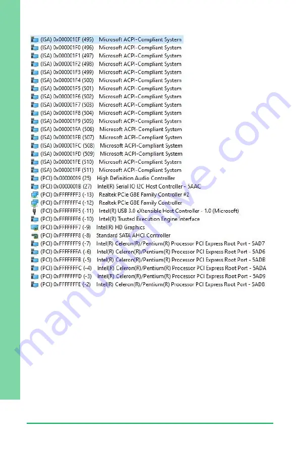
Page 101: ...Appendix A I O Information 87 3 5 Subcompact Board GENE APL7 A11 A 3 IRQ Mapping Chart ...

Page 102: ...Appendix A I O Information 88 3 5 Subcompact Board GENE APL7 A11 ...

Page 103: ...Appendix A I O Information 89 3 5 Subcompact Board GENE APL7 A11 ...

Page 104: ...Appendix A I O Information 90 3 5 Subcompact Board GENE APL7 A11 ...

Page 105: ...Appendix A I O Information 91 3 5 Subcompact Board GENE APL7 A11 ...

Page 106: ...Appendix A I O Information 92 3 5 Subcompact Board GENE APL7 A11 ...

Page 107: ...Appendix A I O Information 93 3 5 Subcompact Board GENE APL7 A11 ...

Page 108: ...Appendix A I O Information 94 3 5 Subcompact Board GENE APL7 A11 ...

Page 109: ...Appendix A I O Information 95 3 5 Subcompact Board GENE APL7 A11 ...

Page 110: ...Appendix A I O Information 96 3 5 Subcompact Board GENE APL7 A11 ...

Page 111: ...Appendix A I O Information 97 3 5 Subcompact Board GENE APL7 A11 ...

Page 112: ...3 5 Subcompact Board GENE APL7 A11 Appendix B Appendix B Mating Connectors ...

Page 113: ...able 1709100254 CN9 CN11 Speaker Molex 51021 0200 N A N A CN12 CN13 CN14 CN15 CN16 CN19 CN20 CN21 CN25 CN26 COM Molex 51021 0900 UART Wafer Cable 1701090150 JP6 Front Panel Molex 51110 1050 N A N A CN24 DIO Molex 51110 1050 N A N A CN28 RTC Battery Molex 51021 0200 Battery Cable 175011901C CN29 CN36 USB Molex 51021 0500 USB Wafer Cable 1700050207 CN27 SATA PWR JST PHR 2 2 Pins for SATA Power 17021...

Reviews: