background image


                TSD 

  Lv3Lv4 Repair Manual


ASUS M530w Level 3 & 

Level 4 Service Manual 


ASUS Proprietary 

1

Summary of Contents for M530w

Page 1: ...TSD Lv3Lv4 Repair Manual 華 華碩 碩電 電腦 腦 ASUS M530w Level 3 Level 4 Service Manual ASUS Proprietary 1 ...

Page 2: ...scilloscope 11 3 3 USB Download Cable 11 3 4 Earpiece 11 3 5 PC 11 4 DOWNLOAD PROCEDURE 12 4 1 Introduction 12 4 2 Operation procedure 12 4 3 Repair method 13 5 LCM DISPLAY 14 5 1 Introduction 14 5 2 Measure method 15 5 3 Repair method 15 6 USB CHARGING 16 6 1 Introduction 16 6 2 Repair method 16 7 KEYPAD 17 7 1 Introduction 17 7 2 Measure method 20 7 3 Repair method 20 ASUS Proprietary 2 ...

Page 3: ...CS 26 10 1 HANDSET 26 10 1 1 Introduction 26 10 1 2 Measure method 28 10 1 3 Repair method 28 10 2 EARPIECE 30 10 2 1 Introduction 30 10 2 2 Measure method 30 10 2 3 Repair method 31 11 CAMERA 32 Introduction 32 11 1 2M camera 32 11 1 1 Measure method 32 11 1 2 Repair method 33 11 2 VGA camera 33 11 2 1 Measure method 34 11 2 2 Repair method 34 12 SIM INTERFACE 35 12 1 Introduction 35 ASUS Proprie...

Page 4: ...troduction 37 14 2 Measure method 37 14 3 Repair method 38 15 RF REPAIR EQUIPMENT REQUIREMENTS 39 15 1 Software requirements 39 15 2 Hardware requirements 39 15 3 Instrument requirements 39 15 4 Test Environments Setup 41 15 4 1 Instrument linking 41 15 4 2 Fixture 42 16 RF BLOCK DIAGRAM 43 16 1 GSM block diagram 43 16 2 WCDMA block diagram 44 17 RF TX RX PATH AND TEST POINTS 45 ASUS Proprietary 4...

Page 5: ...AIR 50 18 1 RF repair s procedure 50 18 2 Calibration and pretest error codes for debug 52 19 GENERAL RF DEBUG 61 19 1 General GSM Tx debug 61 19 2 General GSM Rx debug 70 19 3 General WCDMA Tx debug 77 19 4 General WCDMA Rx debug 84 20 APPENDIX 88 20 1 GSM WCDMA wireless test 88 20 2 Bluetooth test 90 20 3 WiFi test 92 ASUS Proprietary 5 ...

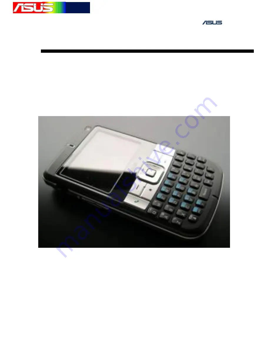
Page 6: ...TSD Lv3Lv4 Repair Manual 華 華碩 碩電 電腦 腦 1 APPEARANCE 1 1 BOX APPEARANCE ASUS Proprietary 6 ...

Page 7: ...TSD Lv3Lv4 Repair Manual 華 華碩 碩電 電腦 腦 1 2 MAIN COMPONENT NAME LOCATION Main Board TOP LAYER 3 4 1 2 5 6 7 8 1 Application CPU Bulverde PXA270 U1 ASUS Proprietary 7 ...

Page 8: ... Lv3Lv4 Repair Manual 華 華碩 碩電 電腦 腦 2 Communication CPU Hermon PXA900 U17 3 PSRAM MT45W1MW16PDGA 70WT U18 4 Cedar Creak U19 5 6 SDRAM U2 U3 7 NAND FLASH M Systems H3 U4 8 PMIC DA9030 U20 ASUS Proprietary 8 ...

Page 9: ...TSD Lv3Lv4 Repair Manual 華 華碩 碩電 電腦 腦 Main Board BOTTOM LAYER TP83 TP82 TP36 TP75 TP50 TP74 TP40 TP7 TP90 TP92 TP89 TP46 TP35 TP47 TP91 TP34 TP88 TP87 TP84 TP86 TP85 TP33 ASUS Proprietary 9 ...

Page 10: ... NAND Flash Dual Camera 2M VGA FPC type Battery Bulverde power CSR BC 04 BT Discrete TPBGA Micro SD push type USB Headset Jack VCHG HMN USB Micron PSRAM Hermon Power speaker M Systems H3 320X240 Landscape LCD UART USB Audio MIC Speaker Receiver Cedar Creek Codec AFE PMIC Arava RF Circuit SIM PCM B T _ U A R T MSL SSP SSP I2C CIF Headset Amp BVD USB ASUS Proprietary 10 ...

Page 11: ... short 3 2 Oscilloscope Check the signals waveforms and voltage levels 3 3 USB Download Cable The software bin file can be downloaded into the handset by the M530w USB download cable The PC also can connect to the handset by it USB Download Cable 3 4 Earpiece The earpiece can be used for the audio loop test 3 5 PC Install the download tool first and execute the download tool ASUS Proprietary 11 ...

Page 12: ... flash The download path is built up by the USB to Serial port download cable 4 2 Operation procedure 1 Set up the power supply voltage and current at 4V and 1A Connect to the battery connector positive and negative of the handset 2 Press the POWER ON Key and Down button The handset would power up and enter the download mode Power on key Down button ASUS Proprietary 12 ...

Page 13: ...n to burn image 4 3 Repair method 1 Check if the USB Connector is soldered poorly or short 2 Check if the fuse F5 blew 3 Check if the U2 U3 and U4 Flash SDRAM chips are placed inversely soldered poorly or short 4 Check if the voltages VCC_SDRAM 1 8V and VCC_NFIO 1 8V are fed the SDRAM and NAND flash If the VCC_SDRAM and VCC_NFIO are abnormal try to change a new DA9030 Power IC ASUS Proprietary 13 ...

Page 14: ...LK_BUF 2 1 L203 600Ohm 100Mhz LCD_GND_2 1 2 3 4 5 6 P N Q13 FDG6331L_NL LCD_B5 LCD_R2 LCD_R0 LCD_G1 LCD_G4 LCD_G2 LCD_G3 LCD_G5 LCD_G0 1 2 R 10 235 KOhm BVD_G0 BVD_B4 BVD_B3 BVD_B1 LCD_R3 LCD_R4 LCD_R1 LCD_R5 BVD_G5 BVD_B2 BVD_B4 BVD_R4 BVD_R3 BVD_R1 BVD_G4 BVD_G2 1 2 R234 220KOhm BVD_B0 BVD_R2 BVD_G1 BVD_G3 BVD_R0 BVD_R4 LCD_B1 LCD_B0 LCD_B4 LCD_B3 LCD_B2 VLCD_2V8 1 2 C220 1000PF 50V SS_RC_3 GND ...

Page 15: ...ay and Black and watch the color 5 3 Repair method 1 When it does Black Screen check if the LCM connector soldered poorly or short 2 When it does White or Black Screen check if the LCM FPC oblique or LCM connector no mounted properly 3 When it does White Screen please check if the U27 is soldered poorly or short 4 When the backlight is no function please check if the MAX8595ZETA U12 C208 C210 C211...

Page 16: ... H 1 2 C207 33PF 50V 1 2 D202 V9MLA0402LWH 1 2 C203 1UF 25V 1 2 C205 33PF 50V 1 1 2 2 3 3 4 4 5 5 NP_NC1 6 NP_NC2 7 SIDE1 8 SIDE2 9 SIDE3 10 SIDE4 11 USB1 USB_1X5P 1 2 D204 V 9 M L A 0 4 0 2 L W H 1 2 D205 V 9 M L A 0 4 0 2 L W H 1 2 R205 470KOhm 1 TP34 tpc60t_np_72 GND GND GND GND GND GND GND CON_USBC_D OTG_ID 2 CON_USBC_D OVP_VCHG_VBUS 10 CARKIT_DET 2 GND GND 6 2 Repair method 1 USB Charger cann...

Page 17: ... 1 2 KEY25 B 1 2 KEY26 N 1 2 KEY27 M 1 2 KEY28 1 2 KEY29 Dot 1 2 KEY30 Message 1 2 KEY6 Y 1 2 KEY5 T 1 2 KEY1 Q 1 2 KEY32 Fn 1 2 KEY31 L shift 1 2 KEY33 Space KP_MKIN7 1 2 KEY35 R shift_CAP 1 2 KEY34 1 2 KEY36 Send 1 2 KEY37 Soft L 1 2 KEY38 Home 1 2 KEY39 Soft R 1 2 KEY40 Back 1 2 KEY41 End 1 2 KEY42 OK 1 2 KEY43 Up 1 2 KEY44 Down KP_MKIN1 KP_MKIN6 KP_MKIN4 KP_MKIN3 KP_MKIN2 KP_MKIN5 1 2 KEY45 Le...

Page 18: ...lume Up Volume Down Power_ON OFF PWR_nON_OFF_1 KP_MKIN1_SK 1 2 3 4 5 6 7 SW2 TACT_SWITCH_4P 6 1 2 3 4 5 SW1 TACT_SWITCH_4P 7 1 2 3 4 5 6 7 SW3 TACT_SWITCH_4P GND GND GND KP_MKOUT3 2 KP_MKOUT2 2 PWR_nON_OFF 10 KP_MKIN1 2 Camera GND KP_MKOUT5 2 KP_MKOUT5_SK 1 2 R668 0Ohm 1 2 3 4 5 6 7 SW5 TACT_SWITCH_4P KP_MKOUT3_SK KP_MKOUT2_SK GND 1 2 C659 0 01UF 50V Function Key Circuit ASUS Proprietary 18 ...

Page 19: ...KP_MKOUT1 2 KP_MKOUT2 2 KP_MKOUT6 2 LED_DRV2 10 LED_DRV1 10 KP_MKIN7 3 KP_MKIN4 2 KP_MKIN1 2 KP_MKIN5 2 KP_MKIN2 2 KP_MKIN6 2 KP_MKIN0 2 KP_MKIN3 2 KP_MKIN0_1 KP_MKIN2_1 KP_MKIN1_1 KP_MKIN4_1 KP_MKIN3_1 KP_MKIN5_1 KP_MKIN6_1 5 6 R N 1 0 C 1 0 0 K O h m 3 4 R N 1 0 B 1 0 0 K O h m 7 8 R N 1 0 D 1 0 0 K O h m 1 2 R N 1 0 A 1 0 0 K O h m KP_MKIN7_1 Keypad Connector Circuit KP_MKOUT3 KP_MKOUT2 KP_MKOU...

Page 20: ...power on the handset 3 After entering the MMI Test Mode select the Keypad Button test item 4 Press every key to verify if each key is OK 5 Press Soft1 key will leave Keypad Button test therefore Soft1 key need press last 7 3 Repair method 1 When the Keypad are no function check if a Keypad connector CON9 are soldered poorly open or short b Serial Resistors R651 R658 are soldered poorly open or ASU...

Page 21: ...unted properly 2 When the function key and JOG DIAL are no function check if the sw1 sw2 sw3 sw4 sw5 and Keypad connector CON9 are soldered poorly damage or short 3 If the above cases are not found try to change the Keypad or Function Key SW1 SW5 ASUS Proprietary 21 ...

Page 22: ...on If the handset is idle the LED would be turned off for saving power 8 2 Measure method 1 Set up the power supply voltage and current at 4V and 1A Connect to the battery connector positive and negative of the handset 2 Press the POWER ON Key to power on the handset 3 After entering the MMI Test Mode select the Led test item ASUS Proprietary 22 ...

Page 23: ...18 AN_LED22 1 2 R20 150Ohm 1 2 LED2 WHITE 1 2 R12 150Ohm 1 2 R14 150Ohm AN_LED12 1 2 R16 150Ohm AN_LED24 AN_LED2 1 2 LED8 WHITE 1 2 R22 150Ohm 1 2 R1 150Ohm VLDO4_3V2 LED_DRV2 AN_LED1 LED_DRV1 1 2 LED1 WHITE 1 2 R25 0Ohm 1 2 LED4 WHITE AN_LED4 1 2 R4 150Ohm 1 2 LED3 WHITE AN_LED3 1 2 R3 150Ohm 1 2 R7 150Ohm AN_LED7 1 2 LED7 WHITE 1 2 R11 150Ohm AN_LED111 2 LED11 WHITE KEYPAD LED circuit 8 3 Measur...

Page 24: ... negative of the handset 2 Press the POWER ON Key to power on the handset 3 After entering the MMI Test Mode select the set Vibrator test item Press on the vibrator should vibrate umt3_rohm sot_416 VIB_OUT V I B _ M O S _ D VIB_D_AN 1 VBAT 2 R220 5 1Ohm VIB_IN 1 2 D207 1SS400 1 2 R216 0Ohm 2 2 1 2 C213 0 1UF 10V G S D 3 2 1 Q3 SI1012R 1 1 U13 VIBRATOR_2P 1 2 R218 0Ohm VIBRATOR_EN 10 1 R222 100KOhm...

Page 25: ...nual 華 華碩 碩電 電腦 腦 9 3 Repair method 1 Check if the R216 R218 R220 R222 D207 Q3 C213are placed inversely soldered poorly damage open or short 2 If the voltage of each pin is normal change a new vibrator ASUS Proprietary 25 ...

Page 26: ...eadset Utilize the handset earpiece Microphone circuit 1 2 R326 0Ohm Microphone MICOB_IP 1 2 R317 100KOhm 1 1 2 C321 100PF 50V 1 2 C319 100PF 50V 1 2 R319 0Ohm 1 2 C322 10UF 10V 1 2 C324 1UF 10V OUTPUT 1 GAIN CONTROL 2 GND 3 POWER 4 U16 SPM0208HE5 SB 1 2 R318 30KOhm 1 VSS_MIC VLDO13_MICBIAS VSS_CCA VSS_MIC VSS_MIC VSS_MIC MIC2_IN 9 MICAMP_O 9 MIC2_IP 9 1 2 C320 1UF 6 3V 1 2 C323 1UF 6 3V MICOB_VD ...

Page 27: ... 50V 2 1 L307 1400Ohm 1Ghz RE_N_OUT RE_P_OUT 2 1 L306 1400Ohm 1Ghz Receiver 1 2 C339 33PF 50V GND GND Receiver circuit 1 2 C331 27PF 50V 1 2 C326 27PF 50V 1 2 C327 27PF 50V GND GND SP_OUT2 10 SP_OUT1 10 1 2 3 4 5 6 G N D D309 PACDN045YB6 1 1 2 2 CON4 POGO_2PIN GND 2 1 L308 330Ohm 100Mhz 2 1 L309 330Ohm 100Mhz Speaker_IN_P Speaker_IN_N Speaker_CONNECTOR Speaker circuit ASUS Proprietary 27 ...

Page 28: ...he speaker 4 Enter the MMI Test Mode and select the Audio test item Press recode blow the handset microphone hole slightly The blowing voice can be heard form the receiver 5 Enter the MMI Test Mode select the Receiver test item The single tone voice can be heard from the receiver 10 1 3 Repair method 1 When the microphone can t work a check if the microphone circuit are soldered poorly damage or s...

Page 29: ...e main PCB Is the pin stand off oblique c If the above cases are not found change the new speaker 3 When the receiver can t work a check if the receiver circuit are soldered poorly damage or short b Check the contact between the receiver pins and the pads on the main PCB Is the pin oblique sunk c If the above cases are not found change the new receiver ASUS Proprietary 29 ...

Page 30: ...lect the Audio test item Press play The melody can be heard from the earpiece 4 Press recode Blow the microphone hole of the earpiece the sound can be heard from the earpiece AJACK_EAR_R_SW AJACK_EAR_R Earpiece circuit 1 2 R316 30KOhm 1 2 C317 100PF 50V 1 2 R315 0Ohm 1 2 C318 100PF 50V 1 2 R314 200KOhm 1 7 8 1 3 5 2 6 4 NP_NC1 NP_NC2 J1 MINI_JACK_6P 1 2 D302 331K 1 2 D305 331K 2 1 L304 1400Ohm 1Gh...

Page 31: ...Manual 華 華碩 碩電 電腦 腦 10 2 3 Repair method 1 Check if the J1 L304 L305 R314 R315 and U14 are placed inversely soldered poorly damage or short 2 If the above cases are not found change the new Phone Jack ASUS Proprietary 31 ...

Page 32: ...his value during system reset VSS_CCA 1 2 C613 0 1UF 10V GND CAM_LV CAM_PCLK 2M_SCL 2M_MCLK I2C_SDA CAM_FV 2M_SDA CIF_DD7 2 CIF_DD5 2 CIF_DD6 2 CIF_DD4 2 CIF_DD2 2 CIF_DD3 2 CIF_DD1 2 GND CIF_DD0 2 VACT_2V8 GND 2M CAMERA circuit 1 VDD_CAM_2V8 2 VGA_MCLK_EN 2M_MCLK_EN 1 2 R610 330Ohm 1 2 C608 0 01UF 10V 1 2 3 4 8 7 6 5 NC1 COM1 IN2 GND V IN1 COM2 NC2 U23 TS5A23167DCUR VGA_MCLK CIF_MCLK 2 1 C604 1UF...

Page 33: ...ad FPC are impaired 4 If the above cases are not found change the 2M camera 11 2 VGA camera GND VGA CAMERA circuit 1 VGA_SCL 1 2 R619 100KOhm G N D 1 2 2 G N D 2 2 3 1 1 3 3 5 5 7 7 9 9 11 11 13 13 15 15 17 17 19 19 21 21 2 2 4 4 6 6 8 8 10 10 12 12 14 14 16 16 18 18 20 20 CON7 FPC_CON_21P 1 2 R603 0Ohm 1 2 R605 0Ohm 1 2 R607 100KOhm CAM_FV VDD_CAM_2V8 VAA_CAM_2V8 VDD_CAM_2V8 I2C_SCL 2 I2C_SDA 2 C...

Page 34: ... Set up the power supply voltage and current at 4V and 1A Connect to the battery connector positive and negative of the handset 2 Press the POWER ON Key to power on the handset 3 After entering the MMI Test Mode select the VGA Camera test item to enter the preview mode 11 2 2 Repair method 1 Check if the U23 and VGA camera connector CON7 are placed inversely soldered poorly damage or short 2 Measu...

Page 35: ... MMI Test Mode MMI would auto run test item SIM test SIM interface 1 2 C107 2 2PF 50V SIM_CLK 1 2 R105 0Ohm 1 2 R101 0Ohm C1 C1 C2 C2 C3 C3 C5 C5 C6 C6 C7 C7 G N D 1 1 G N D 2 2 G N D 3 3 G N D 4 4 CON103 SIM_CON_6P SIM_VPP GND SIM_CLK_IN SIM_CLK_IN SIM_RST HMN_DVDDF R106 7 5KOHM 2 1 2 C106 22PF SIM_DIO 1 2 C111 22PF 1 2 C108 0 1UF HMN_DVDDF GND 1 1 2 C110 22PF 2 1 2 C109 22PF R107 10KOhm 1 GND 12...

Page 36: ...Ohm uSD_EXIST 1 2 C145 2 2UF 10V GND MICRO SD CARD circuit 13 2 Measure method 1 Plug the micro SD card into the handset 2 Set up the power supply voltage and current at 4V and 1A Connect to the battery connector positive and negative of the handset 3 Press the POWER ON Key to power on the handset 4 After entering the MMI Test Mode MMI would auto run test item SD MMC 13 3 Repair method 3 Check if ...

Page 37: ... U107 MAX1583ZETB 1 2 R108 100KOhm Camera Flash LED Driver 1 2 C113 0 1UF Flash LED 1 2 C112 10UF 1 2 R111 3 24KOhm 1 GND VBAT GND GND CAMFLASH_V CAMFLASH_V 1 2 D101 ZHCS400 CAMF_L0 CAMFLASH_STRB_1 CAMFLASH_V CAMFLASH_V Imov Istb TP109 TPC60B_NP_68 1 Flash light LED circuit 14 2 Measure method 1 Set up the power supply voltage and current at 4V and 1A Connect to the battery connector positive and ...

Page 38: ...r method 1 Check if the U107 LED101 C113 C114 and R109 are placed inversely soldered poorly damage or short 2 Check LED101 Polarity is properly as indicated in figure 2 1 4 3 3 Check Board to Board connector mounted properly short ASUS Proprietary 38 ...

Page 39: ...erformance test tool GSM WCDMA debug tool 15 2 Hardware requirements PCB fixture RF adapter RF cable USB cable 15 3 Instrument requirements PC Wireless communication test set Agilent 8960 R S CMU9020 Anritsu 8820 Spectrum analyzer Span 3 0 GHz RF signal generator up to 3 0 GHz High impedance RF probe with DC block Digital multimeter ASUS Proprietary 39 ...

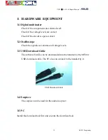
Page 40: ...TSD Lv3Lv4 Repair Manual 華 華碩 碩電 電腦 腦 Power supply ASUS Proprietary 40 ...

Page 41: ...TSD Lv3Lv4 Repair Manual 華 華碩 碩電 電腦 腦 15 4 Test Environments Setup 15 4 1 Instrument linking ASUS Proprietary 41 ...

Page 42: ...TSD Lv3Lv4 Repair Manual 華 華碩 碩電 電腦 腦 15 4 2 Fixture ASUS Proprietary 42 ...

Page 43: ...TSD Lv3Lv4 Repair Manual 華 華碩 碩電 電腦 腦 16 RF Block Diagram 16 1 GSM block diagram ASUS Proprietary 43 ...

Page 44: ...TSD Lv3Lv4 Repair Manual 華 華碩 碩電 電腦 腦 16 2 WCDMA block diagram ASUS Proprietary 44 ...

Page 45: ...Pin12 and Pin13 emit the low band signal GSM900 and high band signals DCS1800 or PCS1900 separately In the low band output signal from RF2722 Pin12 passes through C917 attenuator U903 and RF3166 U904 Pin7 power amplifier sequentially Transmission and receiving switch U902 also named T R switch gets the amplified signal from RF3166 Pin23 via matching circuits RF signal coming from T R switch Pin15 ...

Page 46: ...e output signal which is transmitted from T R switch Pin5 passes through SAW filter BPF4 and matching circuits sequentially Upon RF2722 U901 receiving the signal it is amplified in the Low Noise Amplifier LNA of the receiver down converted the signal s frequency and transformed into IQ signals The IQ signals from RF2722 Pin20 Pin21 Pin22 and Pin23 travel to the transceiver RF6001 U900 The transcei...

Page 47: ...TSD Lv3Lv4 Repair Manual 華 華碩 碩電 電腦 腦 GSM Tx Rx test points ASUS Proprietary 47 ...

Page 48: ...RF signal is radiated via WCDMA antenna of Halley WCDMA Rx path RF signal in WCDMA receiving from base stations via the WCDMA antenna passes through connector Con7 and duplexer Pin3 sequentially MAX2391 Pin1 U958 built in LNA receives the signal from duplexer Then the signal is transmitted to SAW filter BPF6 and returns to receiver MAX2391 again After down converting the signal s frequency and tra...

Page 49: ...TSD Lv3Lv4 Repair Manual 華 華碩 碩電 電腦 腦 WCDMA Tx Rx test points ASUS Proprietary 49 ...

Page 50: ...test engineers can check whether Halley operates properly or not Error codes may occur when calibrating or pretest Haley due to poor RF performance From categorized error codes in the following section engineers can infer the cause of problem by corresponding error codes and find out the defect component by using debug tool There are four kinds of general RF debug including GSM Tx debug GSM Rx deb...

Page 51: ...TSD Lv3Lv4 Repair Manual 華 華碩 碩電 電腦 腦 ASUS Proprietary 51 ...

Page 52: ...k voltage of U904 Pin4 4 Check voltage of U901 Pin24 5 Check voltage of U900 Pin24 47 4206 4208 4209 4210 4211 DCS1800 APC calibration 1 Refer to General GSM Tx debug 2 Check voltage of U902 Pin11 3 Check voltage of U904 Pin4 4 Check voltage of U901 Pin24 5 Check voltage of U900 Pin24 47 4306 4308 4309 4310 4311 PCS1900 APC calibration 1 Refer to General GSM Tx debug 2 Check voltage of U902 Pin11 ...

Page 53: ...5209 5210 5211 5212 5213 5214 DCS1800 AGC calibration 1 Refer to General GSM Rx debug 2 Check voltage of U902 Pin11 3 Check voltage of U901 Pin24 32 4 Check voltage of U900 Pin24 47 5304 5309 5310 5311 5312 5313 5314 PCS1900 AGC calibration 1 Refer to General GSM Rx debug 2 Check voltage of U902 Pin11 3 Check voltage of U901 Pin24 32 4 Check voltage of U900 Pin24 47 ASUS Proprietary 53 ...

Page 54: ...S1 Pin3 3 Rework digital baseband 7006 7010 WCDMA APC calibration 1 Refer to General WCDMA Tx debug 2 Check voltage of U953 Pin1 5 10 3 Check voltage of L21 8005 8009 8013 WCDMA AGC calibration 1 Refer to General WCDMA Rx debug 2 Check voltage of U958 all VCC Pins 10040 10050 WCDMA PD calibration 1 Refer to General WCDMA Tx debug 2 Check voltage of U955 Pin B2 ASUS Proprietary 54 ...

Page 55: ...k voltage of U902 Pin11 3 Check voltage of U904 Pin4 4 Check voltage of U901 Pin24 5 Check voltage of U900 Pin24 47 6 Refer to General GSM Tx debug 7 Rework U902 8 Rework U904 PCS1900 output power 1 Check all RLC on Tx path 2 Check voltage of U902 Pin11 3 Check voltage of U904 Pin4 4 Check voltage of U901 Pin24 5 Check voltage of U900 Pin24 47 6 Refer to General GSM Tx debug 7 Rework U902 8 Rework...

Page 56: ...00 sensitivity 1 Check all RLC on Rx path 2 Check voltage of U902 Pin11 3 Check voltage of U901 Pin24 32 4 Check voltage of U900 Pin24 47 5 Refer to General GSM Rx debug 6 Rework U902 7 Rework BPF3 8 Rework U901 Description Recommendatory Steps GSM900 ORFS 1 Check RLC of low band Tx path 3 Check voltage of U902 Pin11 3 Check voltage of U904 Pin4 4 Check voltage of U901 Pin24 5 Check voltage of U90...

Page 57: ...ltage of U901 Pin24 5 Check voltage of U900 Pin24 47 6 Refer to General GSM Tx debug 7 Rework U902 8 Rework U904 GSM900 RSSI 1 Check all RLC on Rx path 2 Check voltage of U902 Pin11 3 Check voltage of U901 Pin24 32 4 Check voltage of U900 Pin24 47 5 Refer to General GSM Rx debug 6 Rework U902 7 Rework BPF1 8 Rework U901 DCS1800 RSSI 1 Check all RLC on Rx path 2 Check voltage of U902 Pin11 3 Check ...

Page 58: ...of OCS1 Pin3 DCS1800 peak phase error 1 Check voltage of OSC1 Pin1 4 2 Check frequency of OCS1 Pin3 PCS1900 peak phase error 1 Check voltage of OSC1 Pin1 4 2 Check frequency of OCS1 Pin3 GSM900 PVT 1 Format FDI and re calibration 2 Check RLC of low band Tx path 3 Check voltage of U902 Pin11 4 Check voltage of U904 Pin4 5 Check voltage of U901 Pin24 6 Check voltage of U900 Pin24 47 7 Refer to Gener...

Page 59: ...efer to General GSM Tx debug 8 Rework U902 9 Rework U904 PCS1900 PVT 1 Format FDI and re calibration 2 Check RLC of high band Tx path 3 Check voltage of U902 Pin11 4 Check voltage of U904 Pin4 5 Check voltage of U901 Pin24 6 Check voltage of U900 Pin24 47 7 Refer to General GSM Tx debug 8 Rework U902 9 Rework U904 ASUS Proprietary 59 ...

Page 60: ...tage of U958 all VCC Pins WCDMA SEM 1 Refer to General WCDMA Tx debug 2 Check RLC of high band Tx matching 3 Format FDI and re calibration WCDMA ACLR 1 Refer to General WCDMA Tx debug 2 Check RLC of high band Tx matching 3 Format FDI and re calibration WCDMA frequency error 1 Check voltage of OSC1 Pin1 4 2 Check frequency of OCS1 Pin3 3 Rework digital baseband WCDMA EVM 1 Refer to General WCDMA Tx...

Page 61: ...TSD Lv3Lv4 Repair Manual 華 華碩 碩電 電腦 腦 19 General RF Debug 19 1 General GSM Tx debug The flow chart of GSM Tx debug is shown below ASUS Proprietary 61 ...

Page 62: ...MHz 560 5200 PCS 1900 661 0 1880 0 MHz 525 5200 The detail steps of debug are listed as follows GSM 900 Tx debug a Spectrum analyzer connects with a high impedance probe Execute GSM debug tool and set parameters in the above table b Use the high impedance probe to sequentially measure RF power of test points on GSM Tx path including antenna pad L59 C228 and C917 Corresponding locations are shown i...

Page 63: ...t CON6 needs to be reworked if power is measured within 25dBm 32dBm on L59 and no signal is measured from antenna pad The following figure is an example of L59 signal measurement on the spectrum analyzer e C228 Check whether T R switch U902 is good or not T R switch needs to be reworked if power is measured within 25dBm 32dBm on C228 and no signal is measured on L59 The following figure is an exam...

Page 64: ...Bm on C236 and no signal is measured on C228 Besides if no output power is measured on C917 transceiver U900 needs to be reworked The following figure is an example of C917 signal measurement on the spectrum analyzer g The next process returns to calibration and pretest after the defect component is found out and reworked ASUS Proprietary 64 ...

Page 65: ...ng sequential test points the probable defect component should be checked that DC power is supplied for this component at proper voltage level c Antenna pad all components on Tx path are good if power is measured from antenna pad within 25dBm 32dBm In this case engineers shall go to next debug process general GSM Rx debug d L59 Check whether GSM RF connector CON6 is good or not CON6 needs to be re...

Page 66: ... analyzer f C934 Check whether PA U904 is good or not PA needs to be reworked if power is measured within 6dBm 0dBm on C934 and no signal is measured on C234 Besides if no output power is measured on C934 transceiver U900 needs to be reworked The following figure is an example of C934 signal measurement on the spectrum analyzer ASUS Proprietary 66 ...

Page 67: ...na pad L59 C228 and C917 Corresponding locations are shown in 4 RF Tx Rx Path and Test Points Furthermore measurement error of RF power on each test point is unavoidable due to measurement skills and methods of using high impedance probe After probing sequential test points the probable defect component should be checked that DC power is supplied for this component at proper voltage level c Antenn...

Page 68: ...s measured from antenna pad The following figure is an example of L59 signal measurement on the spectrum analyzer e C234 Check whether T R switch U902 is good or not T R switch needs to be reworked if power is measured within 25dBm 32dBm on C228 and no signal is measured on L59 The following figure is an example of C234 signal measurement on the spectrum analyzer ASUS Proprietary 68 ...

Page 69: ...Bm on C934 and no signal is measured on C234 Besides if no output power is measured on C934 transceiver U900 needs to be reworked The following figure is an example of C934 signal measurement on the spectrum analyzer g The next process returns to calibration and pretest after the defect component is found out and reworked ASUS Proprietary 69 ...

Page 70: ...TSD Lv3Lv4 Repair Manual 華 華碩 碩電 電腦 腦 19 2 General GSM Rx debug The flow chart of GSM Rx debug is shown below ASUS Proprietary 70 ...

Page 71: ...0 661 1960 0 MHz 20 dBm The detail steps of debug are listed as follows GSM 900 Rx debug a Set RF signal generator to emit CW with corresponding frequency and transmit power into Halley GSM connector via RF cable and a RF adapter MS 162 Spectrum analyzer connects with a high impedance probe Execute GSM debug tool and set parameters in the above table b Use the high impedance probe to sequentially ...

Page 72: ... emitted by the signal generator is measured on L59 and no power is detected on C869 The following figure is an example of C869 signal measurement on the spectrum analyzer e C868 Check whether SAW filter BPF1 is good or not BPF1 needs to be reworked if RF signal emitted by the signal generator is measured on C869 and no power is detected on C868 The following figure is an example of C868 signal me...

Page 73: ...est points on GSM Rx path including L59 C903 and C895 Corresponding locations are shown in 4 RF Tx Rx Path and Test Points Furthermore measurement error of RF power on each test point is unavoidable due to measurement skills and methods of using high impedance probe After probing sequential test points the probable defect component should be checked that DC power is supplied for this component at ...

Page 74: ...k whether SAW filter BPF4 is good or not BPF4 needs to be reworked if RF signal emitted by the signal generator is measured on C903 and no power is detected on C895 The following figure is an example of C895 signal measurement on the spectrum analyzer f The next process returns to calibration and pretest after the defect component is found out and reworked ASUS Proprietary 74 ...

Page 75: ...oints Furthermore measurement error of RF power on each test point is unavoidable due to measurement skills and methods of using high impedance probe After probing sequential test points the probable defect component should be checked that DC power is supplied for this component at proper voltage level c L59 Check whether GSM RF connector CON6 is good or not CON6 needs to be reworked if no RF sign...

Page 76: ...on C889 and no power is detected on C887 The following figure is an example of C887 signal measurement on the spectrum analyzer f The next process returns to calibration and pretest after the defect component is found out and reworked In a special case receiver U901 needs to be reworked if no problem is found on all Rx paths and pretest is still failed ASUS Proprietary 76 ...

Page 77: ...TSD Lv3Lv4 Repair Manual 華 華碩 碩電 電腦 腦 19 3 General WCDMA Tx debug The flow chart of WCDMA Tx debug is shown below ASUS Proprietary 77 ...

Page 78: ...TSD Lv3Lv4 Repair Manual 華 華碩 碩電 電腦 腦 ASUS Proprietary 78 ...

Page 79: ... component on RF path by using Debug tool Debug tool makes Halley into test mode so that PA can transmit power continuously The usage of debug tool can be referred to Debug tool user guide provided by Halley ATS engineers Related parameters of debug tool are prescribed in the following table UL Channel Tx Frequency Vgc DAC WCDMA 9750 1950 0 MHz 1024 ASUS Proprietary 79 ...

Page 80: ...72 duplexer U956 Pin1 C947 C969 Pin1 C955 L851 Pin1 and L864 Furthermore the signals of C969 Pin1 and L851 Pin1 are both DC signals instead Corresponding locations are shown in 4 RF Tx Rx Path and Test Points Moreover measurement error of RF power on each test point is unavoidable due to measurement skills and methods of using high impedance probe After probing sequential test points the probable ...

Page 81: ...his case engineers shall go to next debug process general WCDMA Rx debug d C972 Check whether WCDMA RF connector CON7 is good or not CON7 needs to be reworked if power is measured within 46dBm 37dBm on C972 and no signal is measured from antenna pad The following figure is an example of C972 signal measurement on the spectrum analyzer ASUS Proprietary 81 ...

Page 82: ...gnal is measured on C972 The following figure is an example of U956 Pin1 signal measurement on the spectrum analyzer f C947 Check whether isolator U954 is good or not CON7 needs to be reworked if power is measured within 46dBm 37dBm on C972 and no signal is measured on U956 Pin1 The following figure is an example of C947 signal measurement on the spectrum analyzer ASUS Proprietary 82 ...

Page 83: ... power h C955 Check whether PA U953 operates normally or not PA needs to be reworked if DC DC converter supplies DC voltage to PA and power is measured within 63dBm 55dBm on C955 The following figure is an example of C955 signal measurement on the spectrum analyzer i L851 Pin1 DC Check whether DC DC converter U951 is good or not The voltage level on L851 Pin1 shall be 2 7V 2 9V as RF power is emit...

Page 84: ...TSD Lv3Lv4 Repair Manual 華 華碩 碩電 電腦 腦 19 4 General WCDMA Rx debug The flow chart of WCDMA Rx debug is shown below ASUS Proprietary 84 ...

Page 85: ...quency and transmit power into Halley WCDMA connector via a RF cable and a RF adapter MS 162 Spectrum analyzer connects with a high impedance probe Execute WCDMA debug tool and set parameters in the above table b Use the high impedance probe to sequentially measure RF power of test points on WCDMA Rx path including C972 C990 C980 and L867 Corresponding locations are shown in 4 RF Tx Rx Path and Te...

Page 86: ...er is measured on C990 The following figure is an example of C990 signal measurement on the spectrum analyzer e C980 Check whether receiver U958 is good or not Receiver needs to be reworked if no power is measured on C980 The following figure is an example of C980 signal measurement on the spectrum analyzer ASUS Proprietary 86 ...

Page 87: ... not BPF6 needs to be reworked if no power is measured on L867 The following figure is an example of L867 signal measurement on the spectrum analyzer g The next process returns to calibration and pretest after the defect component is found out and reworked ASUS Proprietary 87 ...

Page 88: ...TSD Lv3Lv4 Repair Manual 華 華碩 碩電 電腦 腦 20 Appendix 20 1 GSM WCDMA wireless test The flow chart of wireless test is shown below ASUS Proprietary 88 ...

Page 89: ...ng box After that wait for Halley registering at the tester c After attaching to the network make a phone call d Measure maximum output power and sensitivity The test requirements of maximum output power and sensitivity shall not exceed the range listed in the following table e If any of previous steps b d is failed consequently enter next process pretest test f If all previous steps b d are passe...

Page 90: ...TSD Lv3Lv4 Repair Manual 華 華碩 碩電 電腦 腦 20 2 Bluetooth test 1 Open 2577_Bluetooth file 2 Execute autorun 3 Choose TXSTART 24XX which you want ASUS Proprietary 90 ...

Page 91: ...TSD Lv3Lv4 Repair Manual 華 華碩 碩電 電腦 腦 4 Done LCD show Bluetooth Test Mode test mode OK 5 Measure Tx output power with Spectrum analyzer 6 Press ok to leave ASUS Proprietary 91 ...

Page 92: ...TSD Lv3Lv4 Repair Manual 華 華碩 碩電 電腦 腦 20 3 WiFi test 1 Enter Wireless Manager turn on Wi Fi 2 Open Fcctest file 3 Execute FCC Test TX ASUS Proprietary 92 ...

Page 93: ...Lv3Lv4 Repair Manual 華 華碩 碩電 電腦 腦 4 Choose a channel which you want to measure 5 And select Cw TX on test mode OK 6 Measure Tx output power with Spectrum analyzer 7 Select Quit to leave ASUS Proprietary 93 ...

Reviews: