AA280 Motherboard
34
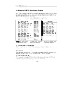
CPU & PCI Bus Control Setup
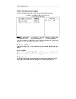
Scroll to this item and press <Enter> to view the following screen:
Phoenix – AwardBIOS CMOS Setup Utility
CPU & PCI Bus Control
Item Help
PCI1 Master 0 WS Write
[Enabled]
PCI2 Master 0 WS Write
[Enabled]
PCI1 Post Write
[Enabled]
PCI2 Post Write
[Enabled]
PCI Delay Transaction
[Disabled]
Menu Level
↑↓→←
:Move
Enter:Select
+/-/PU/PD:Value
F10:Save
ESC:Exit
F1:General Help
F5:Previous Values
F6:Fail-Safe Defaults
F7:Optimized Defaults
Use the arrow keys to navigate through the menu and use the <PgUp> and
<PgDn> to select the desired value for each item.
PCI 1/2 Master 0 WS Write
When enabled, writes to the PCI bus are executed with zero wait states, providing faster data
transfer.
PCI 1/2 Post Write
When enabled, writes from the CPU to PCU bus are buffered, to compensate for the speed
differences between the CPU and PCI bus. When disabled, the writes are not buffered and the
CPU must wait until the write is complete before starting another write cycle.
PCI Delay Transaction
The mainboard’s chipset has an embedded 32-bit post write buffer to support delay transac-
tions cycles. Select Enabled to support compliance with PCI specification version 2.1.

