background image

Armadillo-9                                       

hardware manual ver.1.02


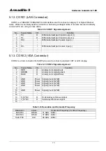
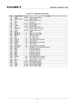
5.12.  CON11 (LAN Connector) 

CON11 is a 10BASE-T/100BASE-TX LAN interface used to connect a category 5 or higher Ethernet 

cable.  While it is normally used to connect to a hub using a straight cable, it can also be used to directly 
connect a PC etc. using a cross-cable. 

Table 5-12 CON11 Signal Assignment 

No. 

Signal Name 

I/O 

Function 

TX+ 

Differential twist pair transmit output (+) 

TX- 

Differential twist pair transmit output (-) 

RX+ 

Differential twist pair receive input (+) 

4 - 

-   

5 - 

-   

RX- 

Differential twist pair receive input (-) 

7 - 

-   

8 - 

-   


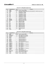
5.13.  CON12 (VGA Connector) 


CON12 is a VGA connector (D-SUB15 pin) used to connect a standard CRT or LCD display. 

Table 5-13 CON12 Signal Assignment 

No. 

Signal Name 

I/O 

Function 

RED 

Analog, color signal (red) 

GREEN 

Analog, color signal (green) 

BLUE 

Analog, color signal (blue) 

4 - 

-  - 

GND 

Power  Signal ground (GND) 

GND 

Power  Signal ground (GND) 

GND 

Power  Signal ground (GND) 

GND 

Power  Signal ground (GND) 

9 - 

-  - 

10 

GND 

Power  Signal ground (GND) 

11 - 

-  - 

12 - 

-  - 

13 H_SYNC 

O  Horizontal synchronous signal 

14 

V_SYNC 

Vertical synchronous signal 

15 - 

-  - 


Table 5-14 Resolution and Horizontal Frequency 

Resolution 

Colors 

Horizontal Frequency (Vertical Frequency) 

640×480 8/16bit 

31.5kHz

60Hz


800×600 8/16bit 

37.9kHz

60Hz


1024×768 8bit 

48.4kHz

60Hz


15

Summary of Contents for Armadillo-9 AN010

Page 1: ...AN010 Hardware Manual Version 1 02 February 21 2005 Atmark Techno Inc http www atmark techno com Armadillo Official Site http armadillo atmark techno com ...

Page 2: ...face 13 5 11 CON10 Compact Flash 14 5 12 CON11 LAN Connector 15 5 13 CON12 VGA Connector 15 5 14 CON13 Power Input Connector 16 5 15 CON14 Extension Power Input 16 5 16 J1 J2 PC 104 Compliant Extension Bus 17 5 16 1 Precautions for PC 104 Extension Bus Access 20 5 16 2 Access Timing 22 5 17 LED D4 23 5 18 LED D5 D6 23 5 19 LED D14 24 5 20 JP1 2 24 5 20 1 JP1 Boot ROM Selection 24 5 20 2 JP2 Boot L...

Page 3: ...12 Table 5 10 CON9 Signal Assignment 13 Table 5 11 CON10 Signal Assignment 14 Table 5 12 CON11 Signal Assignment 15 Table 5 13 CON12 Signal Assignment 15 Table 5 14 Resolution and Horizontal Frequency 15 Table 5 15 CON13 Signal Assignment 16 Table 5 16 CON14 Signal Assignment 16 Table 5 17 J1 Signal Assignment 1 17 Table 5 18 J1 Signal Assignment 2 18 Table 5 19 J2 Signal Assignment 1 19 Table 5 2...

Page 4: ...e 5 4 PC 104 Bus Access Timing 22 Figure 5 5 LED D4 Connections 23 Figure 5 6 LED D5 6 Connections 23 Figure 5 7 LED D14 Connections 24 Figure 5 8 Jumper Connector 25 Figure 6 1 Structure of PC 104 Interrupt Controller 28 Figure 6 2 EXTIRQ Connections 29 Figure 6 3 LED D1 Connections 29 Figure 6 4 Connection of CPU EP9315 and RTC 30 Figure 6 5 Armadillo 9 Power Circuit 30 Figure 7 1 Armadillo 9 Bo...

Page 5: ...ection of I O cards such as memory storage PHS cards and wireless LAN cards Also the PC 104 bus enables functional expansion As the Armadillo 9 employs Linux as its standard operating system you will be able to take advantage of the rich array of open source software resources Software development can be carried out using the GNU assembler C compiler and so on This manual covers the hardware speci...

Page 6: ...duct Board Attachment Detachment Do not attempt to attach or remove this board when power supply is being supplied to the Armadillo 9 or peripheral circuits Static Electricity The Armadillo 9 uses CMOS devices Until the board is used store it safely in the provided antistatic package Latch up Due to excessive noise or surge from the power supply or input output sharp voltage fluctuations can lead ...

Page 7: ...S DTR DSR DCD RI COM2 no flow control pins General Purpose Parallel I O 8 bits 4 bits Timer 16 bit general purpose timer 2 channels one channel used for Linux system timer 32 bit general purpose timer 1 channel 40 bit debug timer 1 channel VGA Connector Type D sub15 pin Max Resolution 1024 768 1024 768 8bit Color 800 600 8 16bit Color 640 480 8 16bit Color USB Host 2 0 Full Speed 12Mbps 1 channel ...

Page 8: ... Max 115 2kbp s Drv Rcv MAX3243 UART2 UART1 Transformer H1102 CON11 RJ45 Ethernet MAC 100BASE TX CON13 5V 3 3V SW Reg LM3485 RTC S 353xxA 4bit 16bit 16bit On Chip Boot ROM Interrupt Controller Timer Parallel I O PLD CoolRunner 64MByte 8MByte Interrupt Control PAS 1 8V PHY LXT97x SW Reg LM3485 EIDE I F CON9 EIDE I F 2mmPitch 44Pin USB0 PCMCIA I F Video LCD Controller CON1 CON2 CON12 VGA CON3 USB A ...

Page 9: ...d 0x4000 0000 0x47FF FFFF Compact Flash I O Space 16bit width 0x4800 0000 0x4BFF FFFF Compact Flash Attribute Space 16bit width 0x4C00 0000 0x4FFF FFFF Compact Flash Memory Space 16bit width 0x5000 0000 0x5FFFFFFF Reserved 0x6000 0000 0x607FFFF Flash Memory 8MByte CS6 16bit width 0x60800000 0x6FFFFFFF Reserved 0x7000 0000 0x7FFF FFFF Reserved 0x8000 0000 0x8008 FFFF EP9315 Internal Register AHB CP...

Page 10: ...6bit width 0xDC00 0000 0xDFFF FFFF Compact Flash Memory Space 16bit width 0xF000 0000 0xF000 000F I O Control Register CS1 8bit width 0xF000 0010 0xF1FF FFFF Reserved 0xF200 0000 0xF200 FFFF PC 104 I O Space 8bit 0xF201 0000 0xF2FF FFFF Reserved 0xF300 0000 0xF3FF FFFF PC 104 Memory Space 8bit 0xF600 0000 0xF600 FFFF PC 104 I O Space 16bit CS2 16bit width 0x F601 0000 0x F6FF FFFF Reserved 0x F700...

Page 11: ...lo 9 s interfaces is shown in Figure 5 1 CON6 CON2 COM2 Compact Flash CON7 LED CON13 Power CON14 Power Ext LED JP1 CON8 Ext CODEC CON10 Compact Flash J1 PC 104 J2 PC 104 D4 IDE JP2 D14 Power CON11 LAN LED D5 D6 LAN CON4 GPIO CON5 GPIO CON9 IDE CON12 VGA CON1 COM1 CON3 USB SW1 RESET Figure 5 1 Interface Layout 7 ...

Page 12: ...Extension Connector stack through No connector LED D4 IDE Access No connector LED D5 6 LAN Access Link Active LED D14 Power Supply No connector JP1 JP2 Boot Mode Setting Jumpers SW1 RESET Switch 5 2 CON1 Serial Interface 1 CON1 is an asynchronous start stop serial interface It is connected to UART1 on the CPU EP9315 Signal input output level RS232C Maximum data rate 115 2kbps Flow Control CTS RTS ...

Page 13: ... to CON2 6 pin on the board loopback 5 TXD O Connects to UART2 TXD pin of EP9315 6 CTS I Connects to CON2 4 pin on the board loopback 7 8 9 GND Power Power supply GND 10 3 3V Power Power supply 3 3V 5 4 CON3 USB Interface CON3 is a USB serial interface It is connected to USB0 on the CPU EP9315 Data Transfer Mode USB2 0 Full Speed 12Mbps Low Speed 1 5Mbps Power Supply Voltage 5V Current 500mA max C...

Page 14: ...PIO port 7 Connects to EGPIO11 Port B 4 pin of EP9315 Electrical specifications of the parallel interface are shown in Table 5 6 Table 5 6 Electrical Specifications of CON4 Parallel Interface Symbol Parameter Min Max Unit Conditions VIH CMOS Input high voltage 0 65 VDDIO VDDIO 0 3 V VDDIO 3 3V VIL CMOS Input low voltage 0 3 0 35 VDDIO V VOH CMOS Output high voltage 2 8 V IOH 4mA VOL CMOS Output lo...

Page 15: ...y 3 3V 2 GND Power Power supply GND 3 TRST I JTAG TRST on EP9315 4 GND Power Power supply GND 5 TDI I JTAG TDI on EP9315 6 GND Power Power supply GND 7 TMS I JTAG TMS on EP9315 8 GND Power Power supply GND 9 TCK I JTAG TCK on EP9315 10 GND Power Power supply GND 11 TDO O JTAG TDO on EP9315 12 Reserved 13 3 3V Power Power supply 3 3V 14 GND Power Power supply GND 5 8 CON7 Normal operation is not gu...

Page 16: ... to Table 5 9 CPU SCLK1 12 GND Power Power supply GND The functionality assigned to the CON8 pins can be switched by setting the EP9315 register Three modes are available Normal Mode I2S on AC97 Mode and I2S on SSP Mode which can be selected by rewriting bit6 I2S on AC97 and bit7 I 2S on SSP of the DeviceCfg Register at 0x8093 0080 Table 5 9 Pin Functionality in Each Mode Pin Name Normal Mode I2S ...

Page 17: ...O Data bus bit12 13 DD2 I O Data bus bit2 14 DD13 I O Data bus bit13 15 DD1 I O Data bus bit1 16 DD14 I O Data bus bit14 17 DD0 I O Data bus bit0 18 DD15 I O Data bus bit15 19 GND Power Power supply GND 20 NC Not supported 21 DMARQ I DMA request 22 GND Power Power supply GND 23 DIOW O I O write enable 24 GND Power Power supply GND 25 DIOR O I O read enable 26 GND Power Power supply GND 27 IORDY I ...

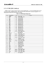
Page 18: ...er Power supply 3 3V 14 A6 O Address bus bit6 15 A5 O Address bus bit5 16 A4 O Address bus bit4 17 A3 O Address bus bit3 18 A2 O Address bus bit2 19 A1 O Address bus bit1 20 A0 O Address bus bit0 21 D0 I O Data bus bit0 22 D1 I O Data bus bit1 23 D2 I O Data bus bit2 24 IOCS16 I I O 16bit 25 CD2 I Card detection 26 CD1 I Card detection 27 D11 I O Data bus bit11 28 D12 I O Data bus bit12 29 D13 I O...

Page 19: ...air receive input 7 8 5 13 CON12 VGA Connector CON12 is a VGA connector D SUB15 pin used to connect a standard CRT or LCD display Table 5 13 CON12 Signal Assignment No Signal Name I O Function 1 RED O Analog color signal red 2 GREEN O Analog color signal green 3 BLUE O Analog color signal blue 4 5 GND Power Signal ground GND 6 GND Power Signal ground GND 7 GND Power Signal ground GND 8 GND Power S...

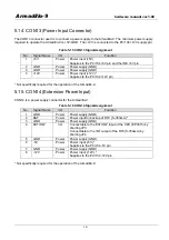
Page 20: ...12V pin Not specifically required for the operation of the Armadillo 9 5 15 CON14 Extension Power Input CON14 is a power supply connector for the Armadillo 9 Table 5 16 CON14 Signal Assignment No Signal Name I O Function 1 GND Power Power supply GND 2 BAT Power Power input for backup of RTC S 353xxA 3 GND Power Power supply GND 4 EXTIRQ I O Connectable to the EXTIRQ input of the CPU EP9315 by shor...

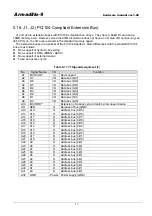
Page 21: ... D7 I O Data bus bit7 A3 D6 I O Data bus bit6 A4 D5 I O Data bus bit5 A5 D4 I O Data bus bit4 A6 D3 I O Data bus bit3 A7 D2 I O Data bus bit2 A8 D1 I O Data bus bit1 A9 D0 I O Data bus bit0 A10 IOCHRDY I Extension of access cycle to match a low speed device A11 AEN O Release of bus GND A12 A19 O Address bus bit19 A13 A18 O Address bus bit18 A14 A17 O Address bus bit17 A15 A16 O Address bus bit16 A...

Page 22: ...I O write strobe B14 IOR O I O read strobe B15 DACK3 O Non support 3 3V pull up B16 DRQ3 I Non support B17 DACK1 O Non support 3 3V pull up B18 DRQ1 I Non support B19 REFRESH O Non support 3 3V pull up B20 SYSCLK O 8 333MHz 1 12 of CPU bus clock B21 IRQ7 I Interrupt request 7 B22 IRQ6 I Interrupt request 6 B23 IRQ5 I Interrupt request 5 B24 IRQ4 I Interrupt request 4 B25 IRQ3 I Interrupt request 3...

Page 23: ...6 D13 I O Data bus bit13 C17 D14 I O Data bus bit14 C18 D15 I O Data bus bit15 C19 KEY GND Table 5 20 J2 Signal Assignment 2 No Signal Name I O Function D0 GND Power Power supply GND D1 MEMCS16 I Non support 5V pull up D2 IOCS16 I Non support 5V pull up D3 IRQ10 I Interrupt request 10 D4 IRQ11 I Interrupt request 11 D5 IRQ12 I Interrupt request 12 D6 IRQ15 I Interrupt request 15 D7 IRQ14 I Interru...

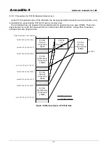
Page 24: ...d 16bit Using either virtual area accesses the same physical area PC 104 I O Physical Area 64kB PC 104 8bit I O Virtual Area 64kB PC 104 16bit I O Virtual Area 64kB 0x0 0xFFFFFF PC 104 8bit Memory Virtual Area 16MB PC 104 Memory Physical Area 16MB 0x0 0xFFFF Hardware Address Linux Address PC 104 16bit Memory Virtual Area 16MB 1 1 8bit Base Address 2 16bit Base Address 2 2 1 0x1200 0000 0x 200 0000...

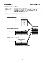
Page 25: ... D15 D0 Accessing the physical areas can be accomplished as follows 8 16 bit Base Address Physical Area offset Address 0x0 0x1 0x2 0x3 0x4 0x5 D0 D7 0x0 0x2 0x4 D0 D7 0x1 0x3 0x5 D8 D15 0x0 0x2 0x4 D0 D7 D8 D15 8bit Base Address 16bit Base Address 16bit Base Address 8bit Physical Area Access 16bit Physical Area 8bit Access 16bit Physical Area 16bit Access 0x0 0x1 0x2 0x3 0x4 0x5 0x6 0x7 Physical A...

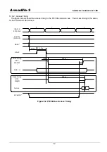
Page 26: ... access timing to the PC 104 extension bus The access timing is the same for both 16bit and 8bit access IOW MEMW ISACLK 8 333MHz IOR MEMR Data out Address A23 A0 BALE Data in IOCHRDY SBHE Write timing Read timing 0 1 2 3 90ns 240ns 240ns 60ns 10ns Figure 5 4 PC 104 Bus Access Timing 22 ...

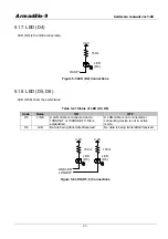
Page 27: ...tatus Table 5 21 Status of LED D5 D6 Code Name ON OFF D5 LINK A LAN cable is connected and a 10BASE T or 100BASE TX link is established A LAN cable is not connected or connecting device is not in active mode D6 LAN Data is being transmitted received No data is being transmitted received 150Ω 3 3V 150Ω 3 3V LINKLED LANLED LED D5 LED D6 Figure 5 6 LED D5 6 Connections 23 ...

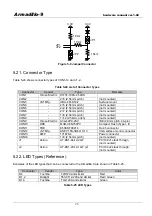
Page 28: ... on board Flash memory For more information on the on chip boot ROM refer to EP9315 User s Guide 5 20 2 JP2 Boot Linux Selection JP2 allows selection of the device storing the Linux Kernel This JP setting is effective only when Linux is installed Table 5 23 Jumper Settings and Function JP1 JP2 Boot Device Boot Kernel OFF OFF On board Flash memory Linux Kernel of on board Flash memory OFF ON On boa...

Page 29: ...m pitch not mounted CON9 Hirose Electric A3A 44PA 2SV IDE 2 0mm pitch 44 pin CON10 DDK MCD CEN750PC Compact Flash Type I II CON11 FRE E5388 F00214 RJ 45 connector CON12 JST Mfg KSEY 15S 3B6L19 13 VGA surface mount connector CON13 AMP 171826 4 Power connector CON14 1 8 2 54mm pitch not mounted J1 Astron AT ES1 64 12 2GF PC 104 J1 stack through not mounted J2 Astron AT ES1 20 12 1GF 2 PC 104 J2 stac...

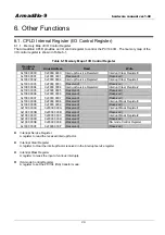
Page 30: ... Clear Register2 0x1000 0005 0xF000 0005 Reserved Reserved 0x1000 0006 0xF000 0006 Reserved Reserved 0x1000 0007 0xF000 0007 Reserved Reserved 0x1000 0008 0xF000 0008 Reserved Interrupt Mask Register0 0x1000 0009 0xF000 0009 Reserved Reserved 0x1000 000A 0xF000 000A Reserved Interrupt Mask Register1 0x1000 000B 0xF000 000B Reserved Reserved 0x1000 000C 0xF000 000C Reserved Interrupt Mask Register2...

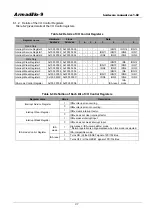
Page 31: ...errupt Mask Register0 0x1000 0008 0xF000 0008 IRQ15 IDE IRQ12 Interrupt Mask Register1 0x1000 000A 0xF000 000A IRQ11 IRQ10 IRQ9 IRQ7 Interrupt Mask Register2 0x1000 000C 0xF000 000C IRQ6 IRQ5 IRQ4 IRQ3 ISA mode Control Register 0x1000 000E 0xF000 000E ISA reset ISA mode Table 6 3 Definition of Each Bit of I O Control Registers Register name Value Description 1 IRQx interrupt is occurring Interrupt...

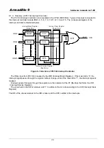
Page 32: ...ster Read Only Interrupt Clear Register Write Only OR ISAINT CPU Figure 6 1 Structure of PC 104 Interrupt Controller The IRQx input from PC 104 is masked by the IMR Interrupt Mask Register If the mask bit is 0 the interrupt signal passes through the register without change while if the mask bit is 1 the interrupt signal is masked Interrupt signals that pass through the register are then retained a...

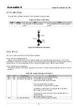
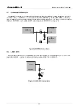
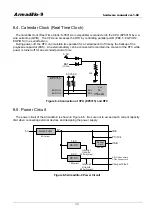
Page 33: ...of IC5 S 353xxA can be sent to outside the board JP3 and JP4 are set to open at shipment Both CPU input signals and IC5 output signals are CMOS3 3V voltage level EP9315 EXTIRQ S 353xxA INT JP4 JP3 CON14 Pin 4 Figure 6 2 EXTIRQ Connections 6 3 LED D1 LED D1 is connected to the PE0 GRLED pin of the CPU EP9315 After functioning as a status LED when internal ROM is booted it can be controlled by setti...

Page 34: ...e connected to maintain the content of the RTC while power is turned off for an extended period of time 3 3V EP9315 EGPIO12 EGPIO13 3 3V S 353xxA SDA SCK 3 3V BAT CON14 Vcc PAS Figure 6 4 Connection of CPU EP9315 and RTC 6 5 Power Circuit The power circuit of the Armadillo 9 is shown in Figure 6 5 Be sure not to exceed each current capacity limit when connecting external devices and designing the ...

Page 35: ...e mounted on some Armadillo 9 models 11 05 10 67 1 6 10 45 3 14 5 75 11 7 4 5 08 6 35 18 0975 26 67 2 54 85 1 90 17 5 08 46 99 25 4 45 085 71 755 90 805 95 885 6 0 6 7 62 23 13 97 5 08 2 54 7 62 10 16 12 7 15 24 39 4 17 9 3 5 74 5 85 0 4 8 8 89 16 51 29 21 34 29 50 165 74 5 82 55 Φ3 2 HOLE Φ6 4 PAD unit mm Figure 7 1 Armadillo 9 Board View 31 ...

Page 36: ...p Table 4 1 Revision of description of External Interrupts Section 6 2 Correction of various typographical errors 1 02 2005 2 21 Correction to CON1 signal assignment description in Table 5 2 Correction to CON5 signal assignment description in Table 5 7 Correction to table in section 5 7 CON6 EP9315 JTAG Correction to CON10 signal assignment description in Table 5 11 Correction of various typograph...

Page 37: ...Armadillo 9 Hardware Manual February 21 2005 version 1 02 Atmark Techno Inc AFT Bldg 6F East 2 North 5 Chuo ku Sapporo Japan 060 0035 TEL011 207 6550 FAX011 207 6570 ...

Reviews: