31
4317I–AVR–01/08
AT90PWM2/3/2B/3B
7.1.5
ADC Clock – clk
ADC
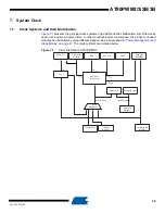
The ADC is provided with a dedicated clock domain. This allows halting the CPU and I/O clocks
in order to reduce noise generated by digital circuitry. This gives more accurate ADC conversion
results.
7.2
Clock Sources
The device has the following clock source options, selectable by Flash Fuse bits as illustrated
Table 7-1. The clock from the selected source is input to the AVR clock generator, and routed to
the appropriate modules.
Note:
1. For all fuses “1” means unprogrammed while “0” means programmed.
The various choices for each clocking option is given in the following sections. When the CPU
wakes up from Power-down or Power-save, the selected clock source is used to time the start-
up, ensuring stable Oscillator operation before instruction execution starts. When the CPU starts
Table 7-1.
Device Clocking Options Select
AT90PWM2/3
Device Clocking Option
CKSEL3..0
External Crystal/Ceramic Resonator
1111 - 1000
Reserved
0111- 0100
PLL output divided by 4 : 16 MHz
0011
Calibrated Internal RC Oscillator
0010
Reserved
0001
External Clock
0000
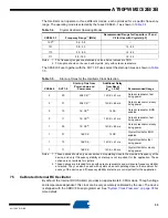
Table 7-2.
Device Clocking Options Select AT90PWM2B/3B
Device Clocking Option
System
Clock
PLL Input
CKSEL3..0
(1)
1.For all fuses “1” means unprogrammed while “0” means programmed
External Crystal/Ceramic Resonator
Ext Osc
(2)
2.Ext Osc : External Osc
RC Osc
(3)
3.RC Osc : Internal RC Oscillator
1111 - 1000
PLL output divided by 4 : 16 MHz / PLL driven by External
Crystal/Ceramic Resonator
Ext Osc
Ext Osc
0100
PLL output divided by 4 : 16 MHz / PLL driven by External
Crystal/Ceramic Resonator
PLL / 4
Ext Osc
0101
Reserved
N/A
N/A
0111- 0110
PLL output divided by 4 : 16 MHz
PLL / 4
RC Osc
0011
Calibrated Internal RC Oscillator
RC Osc
RC Osc
0010
PLL output divided by 4 : 16 MHz / PLL driven by External
clock
PLL / 4
Ext Clk
(4)
4.Ext Clk : External Clock Input
0001
External Clock
Ext Clk
RC Osc
0000


