351
4317I–AVR–01/08
AT90PWM2/3/2B/3B
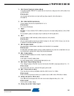
5.
PSC: Output Polarity in Centered Mode
In centered mode, PSCOUTn1 outputs are not inverted, so they are active at the same time
as PSCOUTn0.
Workaround:
Use an external inverter (or a driver with inverting output) to drive the load on
PSCOUTn1.
6.
PSC : POACnA/B Output Activity
These register bits are not implemented in rev A.
Workaround:
Do not use this feature.
7.
VREF
Remark: To have Internal Vref on AREF pin select an internal analog feature such as DAC
or ADC.
Some stand by power consuption may be observed if Vref equals AVcc
8.
DALI
Some troubles on Dali extension when edges are not symmetric.
Workaround:
Use an optocoupler providing symmetric edges on Rx and Tx DALI lines (only recom-
manded for software validation purpose).
9.
DAC: Register Update
Registers DACL & DACH are not written when the DAC is not enabled.
Workaround:
Enable DAC with DAEN before writing in DACL & DACH. To prevent an unwanted zero out-
put on DAC pin, enable DAC output, with DAOE afterwards.
10. DAC : Output spikes
During transition between two codes, a spike may appears
Work around:
Filter spike or wait for steady state
No spike appears if the 4 last signifiant bits remain zero.
11. DAC driver: Output Voltage linearity
The voltage linearity of the DAC driver is limited when the DAC output goes above Vcc - 1V.
Work around:
Do not use AVcc as Vref ; internal Vref gives good results
12. ADC : Conversion accuracy
The conversion accuracy degrades when the ADC clock is 1 & 2 MHz.
Work around:
When a 10 bit conversion accuracy is required, use an ADC clock of 500 kHz or below.
13. Analog comparator: Offset value
The offset value increases when the common mode voltage is above Vcc - 1.5V.
Work around:
Limit common mode voltage
14. Analog comparator: Output signal

