Using the ATEVK525
2-8
ATEVK525 Mass Storage Board for AVR
7740B–AVR–03/08
Table 2-1 .
NAND Flash pin assignment
Note:
The ‘#’ character indicates that the corresponding signal is active low.
2.2.2
Additional devices
NAND Flash Module Description
If another memory device is required for development or evaluation purpose, it is still
possible to install it on the ATEVK525 through an additional module as described below.
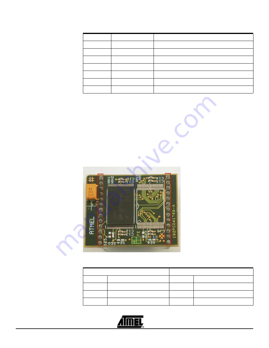
The board provides two SIP-13 receptacle footprints (2.54mm pitch). Users can solder a
receptacle on the board and then insert a NAND Flash module described below, or
directly solder the module.
Figure 2-4 .
NAND Flash module example
Table 2-2 .
NAND Flash module pin-out description
NAND Flash
Microcontroller
Function
I/O[7:0]
PORTA[7:0] (A7-A0)
Data and Address bus
CLE
PORTC0 (A8)
Command Latch Enable
ALE
PORTC1 (A9)
Data Latch Enable
RE#
PORTE1 (RD#)
Read enable
WE#
PORTE0 (WR#)
Write enable
CE#
PORTC2 (A10)
Chip select (active low) (with on-board pull-up)
R/B#
PORTC6
Ready / Busy# (pull-up must be enabled in micro)
NFCON1
NFCON2
Pin #
Function
Pin #
Function
1
WP2#
1
WP3#
2
CE3#
2
R/B3#
3
CE2#
3
R/B2#
1
1
13
13
NFCON1
NFCON2


