230
2467S–AVR–07/09
ATmega128
Analog to
Digital
Converter
Features
•
10-bit Resolution
•
0.5 LSB Integral Non-linearity
•
±2 LSB Absolute Accuracy
•
13 - 260 µs Conversion Time
•
Up to 76.9 kSPS (Up to 15 kSPS at Maximum Resolution)
•
8 Multiplexed Single Ended Input Channels
•
7 Differential Input Channels
•
2 Differential Input Channels with Optional Gain of 10x and 200x
•
Optional Left Adjustment for ADC Result Readout
•
0 - VCC ADC Input Voltage Range
•
Selectable 2.56 V ADC Reference Voltage
•
Free Running or Single Conversion Mode
•
Interrupt on ADC Conversion Complete
•
Sleep Mode Noise Canceler
The ATmega128 features a 10-bit successive approximation ADC. The ADC is connected to an
8-channel Analog Multiplexer which allows 8 single-ended voltage inputs constructed from the
pins of Port F. The single-ended voltage inputs refer to 0V (GND).
The device also supports 16 differential voltage input combinations. Two of the differential inputs
(ADC1, ADC0 and ADC3, ADC2) are equipped with a programmable gain stage, providing
amplification steps of 0 dB (1x), 20 dB (10x), or 46 dB (200x) on the differential input voltage
before the A/D conversion. Seven differential analog input channels share a common negative
terminal (ADC1), while any other ADC input can be selected as the positive input terminal. If 1x
or 10x gain is used, 8-bit resolution can be expected. If 200x gain is used, 7-bit resolution can be
expected.
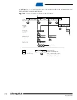
The ADC contains a Sample and Hold circuit which ensures that the input voltage to the ADC is
held at a constant level during conversion. A block diagram of the ADC is shown in
The ADC has a separate analog supply voltage pin, AVCC. AVCC must not differ more than ±
0.3V from V
CC
. See the paragraph
“ADC Noise Canceler” on page 236
on how to connect this
pin.
Internal reference voltages of nominally 2.56V or AVCC are provided On-chip. The voltage refer-
ence may be externally decoupled at the AREF pin by a capacitor for better noise performance.


