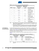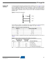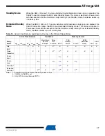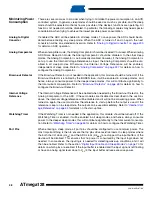
37
2467S–AVR–07/09
ATmega128
Asynchronous Timer
Clock – clk
ASY
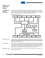
The Asynchronous Timer clock allows the Asynchronous Timer/Counter to be clocked directly
from an external 32 kHz clock crystal. The dedicated clock domain allows using this
Timer/Counter as a real-time counter even when the device is in sleep mode.
ADC Clock – clk
ADC
The ADC is provided with a dedicated clock domain. This allows halting the CPU and I/O clocks
in order to reduce noise generated by digital circuitry. This gives more accurate ADC conversion
results.
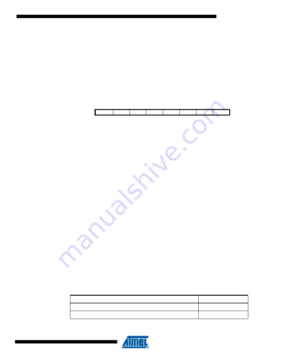
XTAL Divide Control
Register – XDIV
The XTAL Divide Control Register is used to divide the Source clock frequency by a number in
the range 2 - 129. This feature can be used to decrease power consumption when the require-
ment for processing power is low.
• Bit 7 – XDIVEN: XTAL Divide Enable
When the XDIVEN bit is written one, the clock frequency of the CPU and all peripherals (clk
I/O
,
clk
ADC
, clk
CPU
, clk
FLASH
) is divided by the factor defined by the setting of XDIV6 - XDIV0. This bit
can be written run-time to vary the clock frequency as suitable to the application.
• Bits 6..0 – XDIV6..XDIV0: XTAL Divide Select Bits 6 - 0
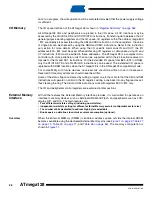
These bits define the division factor that applies when the XDIVEN bit is set (one). If the value of
these bits is denoted
d
, the following formula defines the resulting CPU and peripherals clock
frequency
f
CLK
:
The value of these bits can only be changed when XDIVEN is zero. When XDIVEN is written to
one, the value written simultaneously into XDIV6..XDIV0 is taken as the division factor. When
XDIVEN is written to zero, the value written simultaneously into XDIV6..XDIV0 is rejected. As
the divider divides the master clock input to the MCU, the speed of all peripherals is reduced
when a division factor is used.
When the system clock is divided, Timer/Counter0 can be used with Asynchronous clock only. The fre-
quency of the asynchronous clock must be lower than 1/4th of the frequency of the scaled down Source
clock. Otherwise, interrupts may be lost, and accessing the Timer/Counter0 registers may fail.
Clock Sources
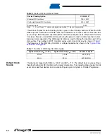
The device has the following clock source options, selectable by Flash fuse bits as shown
below. The clock from the selected source is input to the AVR clock generator, and routed to the
appropriate modules.
Bit
7
6
5
4
3
2
1
0
XDIVEN
XDIV6
XDIV5
XDIV4
XDIV3
XDIV2
XDIV1
XDIV0
XDIV
Read/Write
R/W
R/W
R/W
R/W
R/W
R/W
R/W
R/W
Initial Value
0
0
0
0
0
0
0
0
f
CLK
Source clock
129
d
–
----------------------------------
=
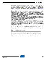
Table 6.
Device Clocking Options Select
Device Clocking Option
CKSEL3..0
External Crystal/Ceramic Resonator
1111 - 1010
External Low-frequency Crystal
1001

