107
2467S–AVR–07/09
ATmega128
Asynchronous
Operation of the
Timer/Counter
Asynchronous Status
Register – ASSR
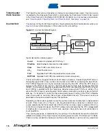
• Bit 3 – AS0: Asynchronous Timer/Counter0
When AS0 is written to zero, Timer/Counter0 is clocked from the I/O clock, clk
I/O
. When AS0 is
written to one, Timer/Counter is clocked from a crystal Oscillator connected to the Timer Oscilla-
tor 1 (TOSC1) pin. When the value of AS0 is changed, the contents of TCNT0, OCR0, and
TCCR0 might be corrupted.
• Bit 2 – TCN0UB: Timer/Counter0 Update Busy
When Timer/Counter0 operates asynchronously and TCNT0 is written, this bit becomes set.
When TCNT0 has been updated from the temporary storage register, this bit is cleared by hard-
ware. A logical zero in this bit indicates that TCNT0 is ready to be updated with a new value.
• Bit 1 – OCR0UB: Output Compare Register0 Update Busy
When Timer/Counter0 operates asynchronously and OCR0 is written, this bit becomes set.
When OCR0 has been updated from the temporary storage register, this bit is cleared by hard-
ware. A logical zero in this bit indicates that OCR0 is ready to be updated with a new value.
• Bit 0 – TCR0UB: Timer/Counter Control Register0 Update Busy
When Timer/Counter0 operates asynchronously and TCCR0 is written, this bit becomes set.
When TCCR0 has been updated from the temporary storage register, this bit is cleared by hard-
ware. A logical zero in this bit indicates that TCCR0 is ready to be updated with a new value.
If a write is performed to any of the three Timer/Counter0 Registers while its update busy flag is
set, the updated value might get corrupted and cause an unintentional interrupt to occur.
The mechanisms for reading TCNT0, OCR0, and TCCR0 are different. When reading TCNT0,
the actual timer value is read. When reading OCR0 or TCCR0, the value in the temporary stor-
age register is read.
Asynchronous
Operation of
Timer/Counter0
When Timer/Counter0 operates asynchronously, some considerations must be taken.
•
Warning: When switching between asynchronous and synchronous clocking of
Timer/Counter0, the Timer Registers TCNT0, OCR0, and TCCR0 might be corrupted. A
safe procedure for switching clock source is:
1.
Disable the Timer/Counter0 interrupts by clearing OCIE0 and TOIE0.
2.
Select clock source by setting AS0 as appropriate.
3.
Write new values to TCNT0, OCR0, and TCCR0.
4.
To switch to asynchronous operation: Wait for TCN0UB, OCR0UB, and TCR0UB.
5.
Clear the Timer/Counter0 interrupt flags.
6.
Enable interrupts, if needed.
•
The Oscillator is optimized for use with a 32.768 kHz watch crystal. Applying an external
clock to the TOSC1 pin may result in incorrect Timer/Counter0 operation. The CPU main
clock frequency must be more than four times the Oscillator frequency.
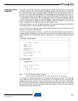
Bit
7
6
5
4
3
2
1
0
–
–
–
–
AS0
TCN0UB
OCR0UB
TCR0UB
ASSR
Read/Write
R
R
R
R
R/W
R
R
R
Initial Value
0
0
0
0
0
0
0
0

