33
ATmega103(L)
0945G–09/01
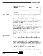
• Bit 1 – OCF0: Output Compare Flag 0
The OCF0 bit is set (one) when compare match occurs between Timer/Counter0 and
the data in OCR0 – Output Compare Register 0. OCF0 is cleared by hardware when
executing the corresponding interrupt handling vector. Alternatively, OCF0 is cleared by
writing a logical “1” to the flag. When the I-bit in SREG and OCIE0 (Timer/Counter2
Compare Interrupt Enable) and the OCF0 are set (one), the Timer/Counter0 Output
Compare interrupt is executed.
• Bit 0 – TOV0: Timer/Counter0 Overflow Flag
The bit TOV0 is set (one) when an overflow occurs in Timer/Counter0. TOV0 is cleared
by hardware when executing the corresponding interrupt handling vector. Alternatively,
TOV0 is cleared by writing a logical “1” to the flag. When the SREG I-bit and TOIE0
(T i m e r / C o u n t e r 0 O v e rf l o w I n t e rr u p t E n a b l e ) a n d T OV 0 a r e s e t ( o n e ), t h e
Timer/Counter0 Overflow interrupt is executed. In PWM mode, this bit is set when
Timer/Counter0 advances from $00.
Interrupt Response Time
The interrupt execution response for all the enabled AVR interrupts is four clock cycles
minimum. Four clock cycles after the interrupt flag has been set, the program vector
address for the actual interrupt handling routine is executed. During this four-clock-cycle
period, the Program Counter (2 bytes) is pushed onto the Stack, and the Stack Pointer
is decremented by 2. The vector is normally a jump to the interrupt routine, and this
jump takes three clock cycles. If an interrupt occurs during execution of a multi-cycle
instruction, this instruction is completed before the interrupt is served.
A return from an interrupt handling routine (same as for a subroutine call routine) takes
four clock cycles. During these four clock cycles, the Program Counter (2 bytes) is
popped back from the stack, and the Stack Pointer is incremented by 2. When the AVR
exits from an interrupt, it will always return to the main program and execute one more
instruction before any pending interrupt is served.
Sleep Modes
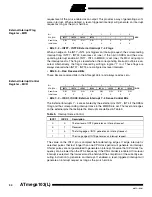
To enter any of the three sleep modes, the SE bit in MCUCR must be set (one) and a
SLEEP instruction must be executed. The SM1 and SM0 bits in the MCUCR register
select which sleep mode (Idle, Power-down, or Power-save) will be activated by the
SLEEP instruction, see Table 3 on page 22.
If an enabled interrupt occurs while the MCU is in a sleep mode, the MCU awakes, exe-
cutes the interrupt routine and resumes execution from the instruction following SLEEP.
The contents of the register file, SRAM, and I/O memory are unaltered. If a reset occurs
during Sleep Mode, the MCU wakes up and executes from the Reset vector.
Idle Mode
When the SM1/SM0 bits are set to 00, the SLEEP instruction makes the MCU enter the
Idle mode, stopping the CPU but allowing SPI, UART, Analog Comparator, ADC,
Timer/Counters, Watchdog and the interrupt system to continue operating. This enables
the MCU to wake up from external triggered interrupts as well as internal ones like the
Timer Overflow and UART Receive Complete interrupts. If wake-up from the Analog
Comparator interrupt is not required, the Analog Comparator can be powered down by
setting the ACD-bit in the Analog Comparator Control and Status Register (ACSR). This
will reduce power consumption in Idle mode. When the MCU wakes up from Idle mode,
the CPU starts program execution immediately.
Power-down Mode
When the SM1/SM0 bits are set to 10, the SLEEP instruction makes the MCU enter the
Power-down mode. In this mode, the external oscillator is stopped while the external
interrupts and the Watchdog (if enabled) continue operating. Only an external reset, a
Watchdog reset (if enabled), or an external level interrupt can wake up the MCU.

