79
ATmega103(L)
0945G–09/01
Interface to External
SRAM
The interface to the SRAM consists of:
Port A: multiplexed low-order address bus and data bus
Port C: high-order address bus
The ALE pin: address latch enable
The RD and WR pin: read and write strobes
The external data SRAM is enabled by setting the external SRAM enable bit (SRE) of
the MCU Control Register (MCUCR) and will override the setting of the data direction
register (DDRA). When the SRE bit is cleared (zero), the external data SRAM is dis-
abled and the normal pin and data direction settings are used. When SRE is cleared
(zero), the address space above the internal SRAM boundary is not mapped into the
internal SRAM as AVR parts do not have an interface to the external SRAM.
When ALE goes from high to low, there is a valid address on Port A. ALE is low during a
data transfer. RD and WR are active when accessing the external SRAM only.
When the external SRAM is enabled, the ALE signal may have short pulses when
accessing the internal RAM, but the ALE signal is stable when accessing the external
SRAM.
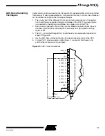
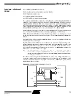
Figure 50 shows how to connect an external SRAM to the AVR using eight latches that
are transparent when G is high.
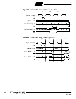
By default, the external SRAM access is a three-cycle scheme as depicted in Figure 51.
When one extra wait state is needed in the access cycle, set the SRW bit (one) in the
MCUCR register. The resulting access scheme is shown in Figure 52. In both cases,
note that Port A is data bus in one cycle only. As soon as the data access finishes, Port
A becomes a low-order address bus again.
Note:
If a read is followed by a write, or vice versa, there is no extra insertion of wait states in
between. The user may insert a NOP between consecutive read and write operations to
the external RAM, because such short time for releasing the bus is difficult to obtain with-
out making bus contention.
For details on the timing for the SRAM interface, please refer to Figure 79, Table 45,
Table 46, Table 47, and Table 48 in the section “DC Characteristics” on page 113 and
refer to “Architectural Overview” on page 8 for a description of the memory map, includ-
ing address space for SRAM.
Figure 50.
External SRAM Connected to the AVR
D[7:0]
A[7:0]
A[15:8]
SRAM
WR
RD
D
Q
G
Port A
ALE
Port C
AVR
RD
WR

