100
ATmega103(L)
0945G–09/01
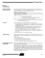
The Flash program memory array on the ATmega103(L) is organized as 512 pages of
256 bytes each. When programming the Flash, the program data is latched into a page
buffer. This allows one page of program data to be programmed simultaneously in either
programming mode.
The EEPROM data memory array on the ATmega103(L) is programmed byte-by-byte in
either programming mode. An auto-erase cycle is provided within the self-timed
EEPROM write instruction in the serial programming mode.
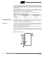
During programming, the supply voltage must be in accordance with Table 36.
Parallel Programming
This section describes how to parallel program and verify Flash program memory,
EEPROM data memory, Lock bits and Fuse bits in the ATmega103(L). Pulses are
assumed to be at least 500 ns unless otherwise noted.
Signal Names
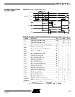
In this section, some pins of the ATmega103(L) are referenced by signal names describ-
ing their function during parallel programming (see Figure 72 and Table 37). Pins not
described in Table 37 are referenced by pin names.
The XA1/XA0 pins determine the action executed when the XTAL1 pin is given a posi-
tive pulse. The bit coding is shown in Table 38.
When pulsing WR or OE, the command loaded determines the action executed. The
command is a byte where the different bits are assigned functions, as shown in Table
39.
Figure 72.
Parallel Programming
Table 36.
Supply Voltage during Programming
Part
Serial Programming
Parallel Programming
ATmega103
4.0 - 5.0V
4.0 - 5.0V
ATmega103L
3.2 - 3.6V
3.2 - 5.0V
ATmega103(L)
VCC
V
CC
PA0
GND
XTAL1
PD1
PD2
PD3
PD4
PD5
PD6
PAGEL
RDY/BSY
OE
BS1
XA0
XA1
WR
PB7 - PB0
DATA
RESET
+12V
PD7


