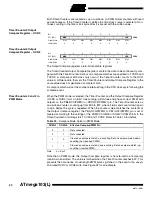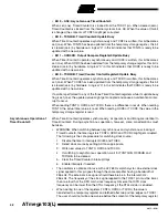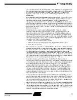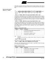
47
ATmega103(L)
0945G–09/01
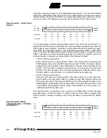
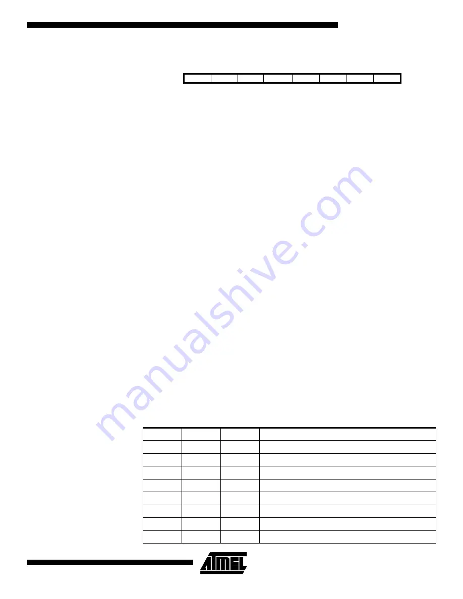
Timer/Counter1 Control
Register B – TCCR1B
• Bit 7 – ICNC1: Input Capture1 Noise Canceler (4 CKs)
When the ICNC1 bit is cleared (zero), the Input Capture Trigger Noise Canceler function
is disabled. The input capture is triggered at the first rising/falling edge sampled on the
input capture pin PD4(IC1) as specified. When the ICNC1 bit is set (one), four succes-
sive samples are measured on PD4(IC1), and all samples must be high/low according to
the input capture trigger specification in the ICES1 bit. The actual sampling frequency is
XTAL clock frequency.
• Bit 6 – ICES1: Input Capture1 Edge Select
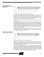
While the ICES1 bit is cleared (zero), the Timer/Counter1 contents are transferred to the
Input Capture Register (ICR1) on the falling edge of the input capture pin – PD4(IC1).
While the ICES1 bit is set (one), the Timer/Counter1 contents are transferred to the
Input Capture Register on the rising edge of the input capture pin – PD4(IC1).
• Bits 5, 4 – Res: Reserved Bits
These bits are reserved bits in the ATmega103(L) and always read as zero.
• Bit 3 – CTC1: Clear Timer/Counter1 on Compare Match
When the CTC1 control bit is set (one), the Timer/Counter1 is reset to $0000 in the clock
cycle after a compareA match. If the CTC1 control bit is cleared, Timer/Counter1 contin-
ues counting and is unaffected by a compare match. Since the compare match is
detected in the CPU clock cycle following the match, this function will behave differently
when a prescaling higher than 1 is used for the timer. When a prescaling of 1 is used
and the compareA register is set to C, the timer will count as follows if CTC1 is set:
... | C-2 | C-1 | C | 0 | 1 | ...
When the prescaler is set to divide by 8, the timer will count like this:
... | C-2, C-2, C-2, C-2, C-2, C-2, C-2, C-2 | C-1, C-1, C-1, C-1, C-1, C-1, C-1, C-1 | C, 0,
0, 0, 0, 0, 0, 0 | ...
In PWM mode, this bit has no effect.
• Bits 2, 1, 0 – CS12, CS11, CS10: Clock Select1, Bits 2, 1 and 0
The lock Select1 bits 2, 1 and 0 define the prescaling source of Timer/Counter1.
Bit
7
6
5
4
3
2
1
0
$2E ($4E)
ICNC1
ICES1
–
–
CTC1
CS12
CS11
CS10
TCCR1B
Read/Write
R/W
R/W
R
R
R/W
R/W
R/W
R/W
Initial Value
0
0
0
0
0
0
0
0
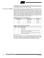
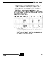
Table 17.
Clock1 Prescale Select
CS12
CS11
CS10
Description
0
0
0
Stop, the Timer/Counter1 is stopped.
0
0
1
CK
0
1
0
CK/8
0
1
1
CK/64
1
0
0
CK/256
1
0
1
CK/1024
1
1
0
External Pin T1, falling edge
1
1
1
External Pin T1, rising edge

