background image

51

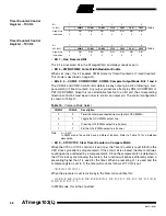
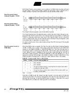
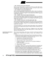
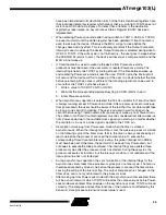
ATmega103(L)

0945G–09/01

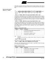
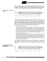
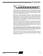
Figure 35.  

Effects on Unsynchronized OCR1 Latching

During the time between the write and the latch operation, a read from OCR1A or
OCR1B will read the contents of the temporary location. This means that the most
recently written value always will read out of OCR1A/B.

When the OCR1A/OCR1B contains $0000 or TOP, the output OC1A/OC1B is updated
t o   l o w   o r   h i g h   o n   t h e   n e x t   c o m p a r e   m a t c h   a c c o r d i n g   t o   t h e   s e t t i n g s   o f
COM1A1/COM1A0 or COM1B1/COM1B0. This is shown in Table 20.

Note:

If the compare register contains the TOP value and the prescaler is not in use
(CS12..CS10 = 001), the PWM output will not produce any pulse at all, because the up-
counting and down-counting value is reached simultaneously. When the prescaler is in
use (CS12..CS10

001 or 000), the PWM output goes active when the counter reaches

the TOP value, but the down-counting compare match is not interpreted to be reached
before the next time the counter reaches the TOP value, making a one-period PWM
pulse.

Note:

X = A or B

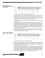
In PWM mode, the Timer Overflow Flag1, TOV1, is set when the counter advances from
$0000. Timer Overflow Interrupt1 operates exactly as in normal Timer/Counter mode,
i.e., it is executed when TOV1 is set provided that Timer Overflow Interrupt1 and global
interrupts are enabled. This does also apply to the Timer Output Compare1 flags and
interrupts.

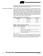
Table 20.  

PWM Outputs OCR1X = $0000 or TOP

COM1X1

COM1X0

OCR1X

Output OC1X

1

0

$0000

L

1

0

TOP

H

1

1

$0000

H

1

1

TOP

L

Counter Value

Compare Value

PWM Output OC1X

Synchronized

OCR1X Latch

Counter Value

Compare Value

PWM Output OC1X

Unsynchronized

OCR1X Latch

Glitch

Compare Value changes

Note: X = A or B

Compare Value changes

Summary of Contents for AVR ATmega103

Page 1: ...Interface Real time Counter RTC with Separate Oscillator Two 8 bit Timer Counters with Separate Prescaler and PWM Expanded 16 bit Timer Counter System with Separate Prescaler Compare Capture Modes and Dual 8 9 or 10 bit PWM Programmable Watchdog Timer with On chip Oscillator 8 channel 10 bit ADC Special Microcontroller Features Low power Idle Power save and Power down Modes Software Selectable Clo...

Page 2: ...8 44 9 43 10 42 11 41 12 40 13 39 14 38 15 37 16 36 17 35 18 34 19 33 PDI RXD PE0 PDO TXD PE1 PEN AC PE2 AC PE3 INT4 PE4 INT5 PE5 INT6 PE6 INT7 PE7 SS PB0 SCK PB1 MOSI PB2 MISO PB3 OC0 PWM0 PB4 PB7 OC2 PWM2 TOSC2 OC1B PWM1B PB6 TOSC1 OC1A PWM1A PB5 PC1 A9 WR PD7 T2 PC2 A10 PC3 A11 PC4 A12 PC5 A13 PC6 A14 PC7 A15 PA7 AD7 ALE PA6 AD6 PA5 AD5 PA4 AD4 PA3 AD3 AD0 PA0 AD1 PA1 AD2 PA2 RD PD6 T1 PD5 PD4 ...

Page 3: ...mer counters with compare modes and PWM UART programmable watchdog timer with internal oscillator an SPI serial port and 3 software selectable power saving modes The Idle mode stops the CPU while allowing the SRAM timer counters SPI port and interrupt system to continue functioning The Power down mode saves the register contents but freezes the oscillator disabling all other chip functions until t...

Page 4: ...A DIR REG PORTD DATA REGISTER PORTB DATA REGISTER PORTE DATA REGISTER PORTA DATA REGISTER PORTC DATA REGISTER PORTD PROGRAMMING LOGIC TIMING AND CONTROL OSCILLATOR OSCILLATOR INTERRUPT UNIT EEPROM SPI UART STATUS REGISTER Z Y X ALU PORTB DRIVER BUFFERS PORTE DRIVER BUFFERS PORTA DRIVER BUFFERS PORTF BUFFERS ANALOG MUX ADC PORTD DRIVER BUFFERS PORTC DRIVERS PB0 PB7 PE0 PE7 PA0 PA7 PF0 PF7 RESET VCC...

Page 5: ...utput only port the Port C pins are not tri stated when a reset condi tion becomes active Port D PD7 PD0 Port D is an 8 bit bi directional I O port with internal pull up resistors The Port D output buffers can sink 20 mA As inputs Port D pins that are externally pulled low will source current if the pull up resistors are activated Port D also serves the functions of various special features The Po...

Page 6: ...ut for the ADC converter For ADC operations a volt age in the range AGND to AVCC must be applied to this pin AGND If the board has a separate analog ground plane this pin should be connected to this ground plane Otherwise connect to GND PEN PEN is a programming enable pin for the serial programming mode By holding this pin low during a power on reset the device will enter the serial programming mo...

Page 7: ... Figure 3 External Clock Drive Configuration Timer Oscillator For the Timer Oscillator pins TOSC1 and TOSC2 the crystal is connected directly between the pins No external capacitors are needed The oscillator is optimized for use with a 32 768 Hz watch crystal Applying an external clock source to TOSC1 is not recommended XTAL2 XTAL1 GND NC EXTERNAL OSCILLATOR SIGNAL ...

Page 8: ...the stack The stack is effectively allocated in the general data SRAM and consequently the stack size is only limited by the total SRAM size and the usage of the SRAM All user programs must initialize the SP in the reset routine before subroutines or interrupts are executed The 16 bit stack pointer SP is read write accessible in the I O space The 4000 bytes data SRAM can be easily accessed through...

Page 9: ...nstruction for load immediate constant data These instructions apply to the second half of the registers in the register file R16 R31 The general SBC SUB CP AND and OR and all other operations between two registers or on a single register apply to the entire register file As shown in Figure 5 each register is also assigned a data memory address mapping them directly into the first 32 locations of ...

Page 10: ...re divided into three main categories arithmetic logical and bit functions ISP Flash Program Memory The ATmega103 L contains 128K bytes of On chip In System Programmable Flash memory for program storage Since all instructions are single or double 16 bit words the Flash is organized as 64K x 16 The Flash memory has an endurance of at least 1000 write erase cycles Constant tables can be allocated in...

Page 11: ... 0020 005F 0000 7FFF FFFF 0FFF 0060 Data Memory Program Memory Program Flash 32K 64K x 16 Memory Configuration A 0000 001F 0020 005F 0000 7FFF FFFF 1000 0FFF FFFF 0060 Program Memory Program Flash 32K 64K x 16 Memory Configuration B 32 Registers 64 I O Registers Internal SRAM 4000 x 8 Data Memory External SRAM 0 64K x 8 ...

Page 12: ...hen external SRAM interface is used with wait state two additional clock cycles are used per byte This has the following effect Data transfer instructions take two extra clock cycles whereas interrupt subroutine calls and returns will need four clock cycles more than specified in the Instruction Set Summary on page 130 The five different addressing modes for the data memory cover Direct Indirect w...

Page 13: ...re 9 Direct Register Addressing Two Registers Operands are contained in registers r Rr and d Rd The result is stored in register d Rd I O Direct Figure 10 I O Direct Addressing Operand address is contained in six bits of the instruction word n is the destination or source register address REGISTER FILE 0 31 d OP d 0 4 15 REGISTER FILE 0 31 d r OP d r 0 4 5 9 15 I O MEMORY 0 63 OP P 0 5 15 n ...

Page 14: ... 12 Data Indirect with Displacement Operand address is the result of the Y or Z register contents added to the address con tained in six bits of the instruction word Data Indirect Figure 13 Data Indirect Addressing Operand address is the contents of the X Y or the Z register OP Rr Rd 16 31 15 0 16 LSBs 0000 FFFF 20 19 Data Space Data Space 0000 FFFF Y OR Z REGISTER OP a n 0 0 5 6 10 15 15 Data Spa...

Page 15: ... X Y or the Z register is incremented after the operation Operand address is the contents of the X Y or the Z register prior to incrementing Constant Addressing Using the LPM and ELPM Instructions Figure 16 Code Memory Constant Addressing Constant byte address is specified by the Z register contents The 15 MSBs select word address 0 32K LSB selects low byte if cleared LSB 0 or high byte if set LSB...

Page 16: ...ate in the instruction words Indirect Program Addressing IJMP and ICALL Figure 18 Indirect Program Memory Addressing Program execution continues at address contained by the Z register i e the PC is loaded with the contents of the Z register Relative Program Addressing RJMP and RCALL Figure 19 Relative Program Memory Addressing OP 16 21 20 31 15 0 16 LSBs PROGRAM MEMORY 0000 7FFF FFFF PROGRAM MEMOR...

Page 17: ...ision is used Figure 20 shows the parallel instruction fetches and instruction executions enabled by the Harvard architecture and the fast access register file concept This is the basic pipe lining concept to obtain up to 1 MIPS per MHz with the corresponding unique results for functions per cost functions per clocks and functions per power unit Figure 20 The Parallel Instruction Fetches and Instr...

Page 18: ...er 3E 5E SPH Stack Pointer High 3D 5D SPL Stack Pointer Low 3C 5C XDIV XTAL Divide Control Register 3B 5B RAMPZ RAM Page Z Select Register 3A 5A EICR External Interrupt Control Register 39 59 EIMSK External Interrupt MaSK register 38 58 EIFR External Interrupt Flag Register 37 57 TIMSK Timer Counter Interrupt MaSK register 36 56 TIFR Timer Counter Interrupt Flag register 35 55 MCUCR MCU General Co...

Page 19: ... Register High 1E 3E EEARL EERPOM Address Register Low 1D 3D EEDR EEPROM Data Register 1C 3C EECR EEPROM Control Register 1B 3B PORTA Data Register Port A 1A 3A DDRA Data Direction Register Port A 19 39 PINA Input Pins Port A 18 38 PORTB Data Register Port B 17 37 DDRB Data Direction Register Port B 16 36 PINB Input Pins Port B 15 35 PORTC Data Register Port C 12 32 PORTD Data Register Port D 11 3...

Page 20: ...ad as set thus clearing the flag The CBI and SBI instructions work with registers 00 to 1F only The different I O and peripherals control registers are explained in the following sections Status Register SREG The AVR status register SREG at I O space location 3F 5F is defined as Bit 7 I Global Interrupt Enable The global interrupt enable bit must be set one for the interrupts to be enabled The ind...

Page 21: ...on page 130 for detailed information Note that the status register is not automatically stored when entering an interrupt rou tine or restored when returning from an interrupt routine This must be handled by software Stack Pointer SP The general AVR 16 bit Stack Pointer is effectively built up of two 8 bit registers in the I O space locations 3E 5E and 3D 5D As the ATmega103 L supports up to 64K b...

Page 22: ...ternal SRAM Wait State When the SRW bit is set one a one cycle wait state is inserted in the external data SRAM access cycle When the SRW bit is cleared zero the external data SRAM access is executed with a three cycle scheme See Figure 51 on page 80 and Figure 52 on page 80 Bit 5 SE Sleep Enable The SE bit must be set one to make the MCU enter the Sleep Mode when the SLEEP instruction is executed...

Page 23: ... divider divides the master clock input to the MCU the speed of all peripherals is reduced when a division factor is used Reset and Interrupt Handling The ATmega103 L provides 23 different interrupt sources These interrupts and the separate reset vector each have a separate program vector in the program memory space All interrupts are assigned individual enable bits that must be set one together w...

Page 24: ... SPI Transfer Complete Handler 0024 jmp UART_RXC UART RX Complete Handler 0026 jmp UART_DRE UDR Empty Handler 7 000C INT5 External Interrupt Request 5 8 000E INT6 External Interrupt Request 6 9 0010 INT7 External Interrupt Request 7 10 0012 TIMER2 COMP Timer Counter2 Compare Match 11 0014 TIMER2 OVF Timer Counter2 Overflow 12 0016 TIMER1 CAPT Timer Counter1 Capture Event 13 0018 TIMER1 COMPA Timer...

Page 25: ...dog timer period expires and the Watchdog is enabled During reset all I O registers except the MCU Status Register are then set to their initial values and the program starts execution from address 0000 The instruction placed in address 0000 must be a JMP absolute jump instruction to the reset handling routine If the program never enables an interrupt source the interrupt vectors are not used and ...

Page 26: ...1 0 00 starts the MCU after 5 CPU clock cycles and can be used when an external clock signal is applied to the XTAL1 pin This setting does not use the WDT oscillator and enables very fast start up from the sleep modes Power down or Power save if the clock signal is present during sleep For details refer to the program ming specification starting on page 99 If the built in start up delay is suffici...

Page 27: ... a reset even if the clock is not running Shorter pulses are not guaranteed to generate a reset When the applied signal reaches the Reset Threshold Voltage VRST on its positive edge the delay timer starts the MCU after the Time out period tTOUT has expired Figure 26 External Reset during Operation VCC RESET TIME OUT INTERNAL RESET tTOUT VPOT VRST VCC RESET TIME OUT INTERNAL RESET tTOUT VPOT VRST V...

Page 28: ... on Reset Flag This bit is set by a Power on Reset A Watchdog Reset or an External Reset will leave this bit unchanged To summarize Table 7 shows the value of these two bits after the three modes of reset To make use of these bits to identify a reset condition the user software should clear both the PORF and EXTRF bits as early as possible in the program Checking the PORF and EXTRF values is done ...

Page 29: ...f priority Note that external level interrupt does not have a flag and will only be remembered for as long as the interrupt condition is active Note that the Status Register is not automatically stored when entering an interrupt rou tine or restored when returning from an interrupt routine This must be handled by software External Interrupt Mask Register EIMSK Bits 7 4 INT7 INT4 External Interrupt...

Page 30: ...INT7 INT4 if the SREG I flag and the corresponding interrupt mask in the EIMSK are set The level and edges on the external pins that activate the interrupts are defined in Table 9 The value on the INTX pin is sampled before detecting edges If edge interrupt is selected pulses that last longer than one CPU clock period will generate an interrupt Shorter pulses are not guaranteed to generate an inte...

Page 31: ...curs i e when the OCF1A bit is set in the Timer Counter Interrupt Flag Register Bit 3 OCIE1B Timer Counter1 Output CompareB Match Interrupt Enable When the OCIE1B bit is set one and the I bit in the Status Register is set one the Timer Counter1 CompareB Match interrupt is enabled The corresponding interrupt at vector 001A is executed if a CompareB match in Timer Counter1 occurs i e when the OCF1B ...

Page 32: ...e set one the Timer Counter1 Capture interrupt is executed Bit 4 OCF1A Output Compare Flag 1A The OCF1A bit is set one when compare match occurs between the Timer Counter1 and the data in OCR1A Output Compare Register 1A OCF1A is cleared by hardware when executing the corresponding interrupt handling vector Alternatively OCF1A is cleared by writing a logical 1 to the flag When the I bit in SREG an...

Page 33: ...Program Counter 2 bytes is popped back from the stack and the Stack Pointer is incremented by 2 When the AVR exits from an interrupt it will always return to the main program and execute one more instruction before any pending interrupt is served Sleep Modes To enter any of the three sleep modes the SE bit in MCUCR must be set one and a SLEEP instruction must be executed The SM1 and SM0 bits in th...

Page 34: ...not be executed Power save Mode When the SM1 SM0 bits are 11 the SLEEP instruction makes the MCU enter the Power save mode This mode is identical to Power down with one exception If Timer Counter0 is clocked asynchronously i e the AS0 bit in ASSR is set Timer Counter0 will run during sleep In addition to the Power down wake up sources the device can also wake up from either Timer Overflow or Outpu...

Page 35: ... pin connection that triggers the counting Timer Counter Prescalers Figure 28 Prescaler for Timer Counter1 and Timer Counter2 For Timer Counters 1 and 2 the four different prescaled selections are CK 8 CK 64 CK 256 and CK 1024 where CK is the CPU clock Observe that CPU clock frequency can be lower than the XTAL frequency if the XTAL divider is enabled For Timer Counters 1 and 2 added selections as...

Page 36: ... is optimized for use with a 32 768 kHz crystal 8 bit Timer Counters T C0 and T C2 Figure 30 shows the block diagram for Timer Counter0 Figure 31 shows the block dia gram for Timer Counter2 Figure 30 Timer Counter0 Block Diagram 8 BIT DATA BUS 8 BIT ASYNCH T C0 DATA BUS ASYNCH STATUS REGISTER ASSR TIMER INT FLAG REGISTER TIFR TIMER COUNTER0 TCNT0 SYNCH UNIT 8 BIT COMPARATOR OUTPUT COMPARE REGISTER...

Page 37: ...ture a high resolution and a high accuracy usage with the lower prescaling opportunities Similarly the high prescaling opportunities make these units useful for lower speed functions or exact timing functions with infrequent actions Both Timer Counters support two Output Compare functions using the output compare registers OCR0 and OCR2 as the data source to be compared to the Timer Counter conten...

Page 38: ...e the Timer Counter is reset to 00 in the CPU clock cycle after a compare match If the control bit is cleared the timer continues counting and is unaffected by a compare match Since the compare match is detected in the CPU clock cycle following the match this function will behave differently when a prescaling higher than 1 is used for the timer When a prescaling of 1 is used and the compare regist...

Page 39: ...mer Counter2 TCNT2 These 8 bit registers contain the value of the Timer Counters Table 11 Timer Counter0 Prescale Select CS02 CS01 CS00 Description 0 0 0 Timer Counter0 is stopped 0 0 1 PCK0 0 1 0 PCK0 8 0 1 1 PCK0 32 1 0 0 PCK0 64 1 0 1 PCK0 128 1 1 0 PCK0 256 1 1 1 PCK0 1024 Table 12 Timer Counter2 Prescale Select CS22 CS21 CS20 Description 0 0 0 Timer Counter2 is stopped 0 0 1 CK 0 1 0 CK 8 0 1...

Page 40: ...uts on the PB4 OC0 PWM0 or PB7 OC2 PWM2 pin The Timer Counter acts as an up down counter counting up from 00 to FF where it turns and counts down again to zero before the cycle is repeated When the counter value matches the contents of the Output Compare register the PB4 OC0 PWM0 or PB7 OC2 PWM2 pin is set or cleared according to the settings of the COM01 COM00 or COM21 COM20 bits in the Timer Cou...

Page 41: ...2 operate exactly as in normal Timer Counter mode i e it is executed when TOV0 or TOV2 is set provided that Timer Overflow interrupt and global interrupts are enabled This also applies to the Timer Out put Compare flags and interrupts The frequency of the PWM will be Timer Clock Frequency divided by 510 Asynchronous Status Register ASSR Bits 7 4 Res Reserved Bits These bits are reserved bits in th...

Page 42: ... occur When reading TCNT0 OCR0 and TCCR0 there is a difference in result When reading TCNT0 the actual timer value is read When reading OCR0 or TCCR0 the value in the temporary storage register is read Asynchronous Operation of Timer Counter0 When Timer Counter0 operates synchronously all operations and timing are identical to Timer Counter2 During asynchronous operation however some consideration...

Page 43: ...r should be aware of the fact that this oscillator might take as long as one second to stabilize The user is advised to wait for at least one second before using Timer Counter0 after power up or wake up from Power down The content of all Timer Counter0 registers must be considered lost after a wake up from Power down due to the unstable clock signal upon start up no matter whether the oscillator i...

Page 44: ...e Timer Counter Interrupt Mask Register TIMSK When Timer Counter1 is externally clocked the external signal is synchronized with the oscillator frequency of the CPU To assure proper sampling of the external clock the minimum time between two external clock transitions must be at least one internal CPU clock period The external clock signal is sampled on the rising edge of the internal CPU clock Th...

Page 45: ...r the input capture Refer to Analog Comparator on page 70 for details on this The ICP pin logic is shown in Figure 34 Figure 34 ICP Pin Schematic Diagram 8 BIT DATA BUS T C1 CONTROL REGISTER B TCCR1B T C1 CONTROL REGISTER A TCCR1A T C1 INPUT CAPTURE REGISTER ICR1 16 BIT COMPARATOR 16 BIT COMPARATOR TIMER COUNTER1 OUTPUT COMPARE REGISTER A TIMER COUNTER1 OUTPUT COMPARE REGISTER B TIMER COUNTER1 TCN...

Page 46: ...ernative function to an I O port the corresponding direc tion control bit must be set one to control an output pin The control configuration is given in Table 15 Note X A or B In PWM mode these bits have a different function Refer to Table 16 for a detailed description Bits 3 2 Res Reserved Bits These bits are reserved bits in the ATmega103 L and always read as zero Bits 1 0 PWM11 PWM10 Pulse Widt...

Page 47: ...Clear Timer Counter1 on Compare Match When the CTC1 control bit is set one the Timer Counter1 is reset to 0000 in the clock cycle after a compareA match If the CTC1 control bit is cleared Timer Counter1 contin ues counting and is unaffected by a compare match Since the compare match is detected in the CPU clock cycle following the match this function will behave differently when a prescaling highe...

Page 48: ...are written to the TCNT1 Timer Counter1 register simultaneously Consequently the high byte TCNT1H must be accessed first for a full 16 bit register write operation When using Timer Counter1 as an 8 bit timer it is sufficient to write the low byte only TCNT1 Timer Counter1 Read When the CPU reads the low byte TCNT1L the data of TCNT1L is sent to the CPU and the data of the high byte TCNT1H is place...

Page 49: ...ICR1 If the main program and interrupt routines perform access to registers using TEMP interrupts must be dis abled during access from the main program Timer Counter1 Input Capture Register ICR1H and ICR1L The Input Capture Register is a 16 bit read only register When the rising or falling edge according to the input capture edge setting ICES1 of the signal at the input capture pin PD4 IC1 is dete...

Page 50: ...C1A PB6 OC1B pins are set or cleared according to the settings of the COM1A1 COM1A0 or COM1B1 COM1B0 bits in the Timer Counter1 Control Register TCCR1A Refer to Table 19 for details Note X A or B Note that in the PWM mode the 10 least significant OCR1A OCR1B bits when written are transferred to a temporary location They are latched when Timer Counter1 reaches the value TOP This prevents the occurr...

Page 51: ...aler is in use CS12 CS10 001 or 000 the PWM output goes active when the counter reaches the TOP value but the down counting compare match is not interpreted to be reached before the next time the counter reaches the TOP value making a one period PWM pulse Note X A or B In PWM mode the Timer Overflow Flag1 TOV1 is set when the counter advances from 0000 Timer Overflow Interrupt1 operates exactly as...

Page 52: ...the description of the Watchdog Timer Control Register for details Figure 36 Watchdog Timer Watchdog Timer Control Register WDTCR Bits 7 5 Res Reserved Bits These bits are reserved bits in the ATmega103 L and will always read as zero Bit 4 WDTOE Watchdog Turn off Enable This bit must be set one when the WDE bit is cleared Otherwise the Watchdog will not be disabled Once set hardware will clear thi...

Page 53: ...ristics section The WDR Watchdog Reset instruction should always be executed before the Watchdog Timer is enabled This ensures that the reset period will be in accordance with the Watchdog Timer prescale settings If the Watchdog Timer is enabled without reset the Watchdog Timer may not start counting from zero To avoid unintentional MCU reset the Watchdog Timer should be disabled or reset before c...

Page 54: ...7 0 EEPROM Data For the EEPROM write operation the EEDR register contains the data to be written to the EEPROM in the address given by the EEAR register For the EEPROM read opera tion the EEDR contains the data read out from the EEPROM at the address given by EEAR EEPROM Control Register EECR Bits 7 4 Res Reserved Bits These bits are reserved bits in the ATmega103 L and will always be read as zero...

Page 55: ...tion An interrupt between step 4 and step 5 will make the write cycle fail since the EEPROM Master Write Enable will time out If an interrupt routine accessing the EEPROM is interrupting another EEPROM access the EEAR and EEDR registers will be modified causing the interrupted EEPROM access to fail It is recommended to have the global interrupt flag cleared during the four last steps to avoid thes...

Page 56: ...ROM data corruption can easily be avoided by following these design recommen dations one is sufficient 1 Keep the AVR RESET active low during periods of insufficient power supply voltage This is best done by an external low VCC Reset Protection circuit often referred to as a Brown out Detector BOD Please refer to application note AVR 180 for design considerations regarding power on reset and low v...

Page 57: ... in the master mode and is the clock input in the slave mode Writing to the SPI Data Register of the master CPU starts the SPI clock generator and the data written shifts out of the PB2 MOSI pin and into the PB2 MOSI pin of the slave CPU After shifting one byte the SPI clock generator stops setting the end of transmission flag SPIF If the SPI interrupt enable bit SPIE in the SPCR regis ter is set ...

Page 58: ... sys tem interprets this as another master selecting the SPI as a slave and starts to send data to it To avoid bus contention the SPI system takes the following actions 1 The MSTR bit in SPCR is cleared and the SPI system becomes a slave As a result of the SPI becoming a slave the MOSI and SCK pins become inputs 2 The SPIF flag in SPSR is set and if the SPI interrupt is enabled and the I bit in SR...

Page 59: ...terrupts are enabled Bit 6 SPE SPI Enable When the SPE bit is set one the SPI is enabled and SS MOSI MISO and SCK are connected to pins PB0 PB1 PB2 and PB3 Bit 5 DORD Data Order When the DORD bit is set one the LSB of the data word is transmitted first When the DORD bit is cleared zero the MSB of the data word is transmitted first MSB 6 5 4 3 2 1 LSB 1 2 3 4 5 6 7 8 MSB 6 5 4 3 2 1 LSB SCK CYCLE F...

Page 60: ...e lower than the XTAL frequency if the XTAL divider is enabled SPI Status Register SPSR Bit 7 SPIF SPI Interrupt Flag When a serial transfer is complete the SPIF bit is set one and an interrupt is gener ated if SPIE in SPCR is set one and global interrupts are enabled SPIF is cleared by hardware when executing the corresponding interrupt handling vector Alternatively the SPIF bit is cleared by fir...

Page 61: ...a transfer between the regis ter file and the SPI Shift Register Writing to the register initiates data transmission Reading the register causes the Shift Register Receive buffer to be read Bit 7 6 5 4 3 2 1 0 0F 2F MSB LSB SPDR Read Write R W R W R W R W R W R W R W R W Initial Value X X X X X X X X Undefined ...

Page 62: ...tten to UDR after the stop bit from the previous character has been shifted out The shift register is loaded immediately A new character has been written to UDR before the stop bit from the previous character has been shifted out The shift register is loaded when the stop bit of the character currently being transmitted has been shifted out If the 10 11 bit Transmit Shift register is empty data is...

Page 63: ...fter the stop bit has been present on TXD for one bit length the TX Complete Flag TXC in USR is set The TXEN bit in UCR enables the UART transmitter when set one When this bit is cleared zero the PE1 pin can be used for general I O When TXEN is set the UART transmitter will be connected to PE1 which is forced to be an output pin regardless of the setting of the DDE1 bit in DDRE DATA BUS DATA BUS U...

Page 64: ... as a noise spike and the receiver starts looking for the next 1 to 0 transition If however a valid start bit is detected sampling of the data bits following the start bit is performed These bits are also sampled at samples 8 9 and 10 The logical value found in at least two of the three samples is taken as the bit value All bits are shifted into the transmitter shift register as they are sampled S...

Page 65: ...ceived a character the UDR register has not been accessed since the last receive the OverRun OR flag in USR is set This means that the new data trans ferred to the shift register could not be transferred to UDR and is lost The OR bit is buffered and is available when the valid data byte in UDR has been read The user should always check the OR after reading from the UDR register in order to detect ...

Page 66: ...ransmitting application must enter receive mode and free the communications bus immediately after completing the transmission When the TXCIE bit in UCR is set setting of TXC causes the UART Transmit Complete interrupt to be executed TXC is cleared by hardware when executing the corresponding interrupt handling vector Alternatively the TXC bit is cleared zero by writing a logical 1 to the bit Bit 5...

Page 67: ...ting of the UDRE bit in USR will cause the UART Data Register Empty Interrupt routine to be executed provided that global interrupts are enabled Bit 4 RXEN Receiver Enable This bit enables the UART receiver when set one When the receiver is disabled the RXC OR and FE status flags cannot become set If these flags are set turning off RXEN does not cause them to be cleared Bit 3 TXEN Transmitter Enab...

Page 68: ...rystal frequencies the most commonly used baud rates can be generated by using the UBRR settings in Table 24 Observe that CPU clock frequency can be lower than the XTAL frequency if the XTAL divider is enabled UBRR values that yield an actual baud rate differing less than 2 from the target baud rate are in boldface in the table However using baud rates that have more than 1 error is not recommende...

Page 69: ...RR 47 0 0 UBRR 51 0 2 UBRR 59 0 0 9600 UBRR 20 1 6 UBRR 23 0 0 UBRR 25 0 2 UBRR 29 0 0 14400 UBRR 13 1 6 UBRR 15 0 0 UBRR 16 2 1 UBRR 19 0 0 19200 UBRR 10 3 1 UBRR 11 0 0 UBRR 12 0 2 UBRR 14 0 0 28800 UBRR 6 1 6 UBRR 7 0 0 UBRR 8 3 7 UBRR 9 0 0 38400 UBRR 4 6 3 UBRR 5 0 0 UBRR 6 7 5 UBRR 7 6 7 57600 UBRR 3 12 5 UBRR 3 0 0 UBRR 3 7 8 UBRR 4 0 0 76800 UBRR 2 12 5 UBRR 2 0 0 UBRR 2 7 8 UBRR 3 6 7 115...

Page 70: ... reduce power con sumption in active and idle mode When changing the ACD bit the Analog Comparator interrupt must be disabled by clearing the ACIE bit in ACSR Otherwise an interrupt can occur when the bit is changed Bit 6 Res Reserved Bit This bit is a reserved bit in the ATmega103 L and will always read as zero Bit 5 ACO Analog Comparator Output ACO is directly connected to the comparator output ...

Page 71: ...log comparator and the Input Capture function is given To make the comparator trigger the Timer Counter1 Input Capture interrupt the TICIE1 bit in the Timer Interrupt Mask Register TIMSK must be set one Bits 1 0 ACIS1 ACIS0 Analog Comparator Interrupt Mode Select These bits determine which comparator events that trigger the Analog Comparator inter rupt The different settings are shown in Table 25 ...

Page 72: ...el during conversion A block diagram of the ADC is shown in Figure 45 The ADC has two separate analog supply voltage pins AVCC and AGND AGND must be connected to GND and the voltage on AVCC must not differ more than 0 3V from VCC See the section ADC Noise Canceling Techniques on page 77 on how to connect these pins An external reference voltage must be applied to the AREF pin This voltage must be ...

Page 73: ...same result when they are read This mechanism works as follows When reading data ADCL must be read first Once ADCL is read ADC access to data registers is blocked This means that if ADCL has been read and a conversion com pletes before ADCH is read none of the registers are updated and the result from the conversion is lost When ADCH is read ADC access to the ADCH and ADCL registers is re enabled ...

Page 74: ...iod the ADC will start the new conversion immediately For a summary of conversion times see Table 26 Figure 47 ADC Timing Diagram First Conversion Figure 48 ADC Timing Diagram Table 26 ADC Conversion Time Condition Sample Cycle Number Result Ready Cycle Number Total Conversion Time Cycles Total Conversion Time µs 1st Conversion 14 26 28 140 560 Single Conversion 1 13 15 75 300 MSB of result LSB of...

Page 75: ...Turning the ADC off while a conversion is in progress will terminate this conversion Bit 6 ADSC ADC Start Conversion A logical 1 must be written to this bit to start each conversion The first time ADSC has been written after the ADC has been enabled or if ADSC is written at the same time as the ADC is enabled a dummy conversion will precede the initiated conversion This dummy conversion performs i...

Page 76: ...t Enable When this bit is set one and the I bit in SREG is set one the ADC Conversion Com plete interrupt is activated Bits 2 0 ADPS2 ADPS0 ADC Prescaler Select Bits These bits determine the division factor between the XTAL frequency and the input clock to the ADC ADC Data Register ADCL and ADCH When an ADC conversion is complete the result is found in these two registers It is essential that both...

Page 77: ...he PCB 2 Keep analog signal paths as short as possible Make sure analog tracks run over the analog ground plane and keep them well away from high speed switching digital tracks 3 The AVCC pin on the ATmega103 L should have its own decoupling capacitor as shown in Figure 49 4 Use the ADC Noise Canceler function to reduce induced noise from the CPU 5 If some Port F pins are used as digital inputs it...

Page 78: ...Hz 1 2 LSB Absolute accuracy VREF 4V VCC 4V ADC clock 1 MHz 4 LSB Absolute accuracy VREF 4V VCC 4V ADC clock 2 MHz 16 LSB Integral Non linearity VREF 2V 0 5 LSB Differential Non linearity VREF 2V 0 5 LSB Zero Error Offset 1 LSB Conversion Time 70 280 µs Clock Frequency 50 200 kHz AVCC Analog Supply Voltage VCC 0 3 1 VCC 0 3 2 V VREF Reference Voltage 2 AVCC V RREF Reference Input Resistance 6 10 1...

Page 79: ...table when accessing the external SRAM Figure 50 shows how to connect an external SRAM to the AVR using eight latches that are transparent when G is high By default the external SRAM access is a three cycle scheme as depicted in Figure 51 When one extra wait state is needed in the access cycle set the SRW bit one in the MCUCR register The resulting access scheme is shown in Figure 52 In both cases...

Page 80: ...ck Ø ALE WR RD Data Address 7 0 Data Address 7 0 Address 15 8 Address Address Address T1 T2 T3 Prev Address Prev Address Prev Address Data Data Write Read Address Address System Clock Ø ALE WR RD Data Address 7 0 Data Address 7 0 Address 15 8 Address Address Address T1 T2 T3 T4 Prev Address Prev Address Prev Address Data Data Write Read Addr Addr ...

Page 81: ...esses to the byte When Port A is set to the alternate function by the SRE External SRAM Enable bit in the MCUCR MCU Control Register the alternate settings override the data direction register Port A Data Register PORTA Port A Data Direction Register DDRA Port A Input Pins Address PINA The Port A Input Pins address PINA is not a register this address enables access to the physical value on each Po...

Page 82: ...37 and the Port B Input Pins PINB 16 36 The Port B Input Pins address is read only while the Data Register and the Data Direction Register are read write All port pins have individually selectable pull up resistors The Port B output buffers can sink 20 mA and thus drive LED displays directly When pins PB0 to PB7 are used as Table 28 DDAn Effects on Port A Pins DDAn PORTAn I O Pull up Comment 0 0 I...

Page 83: ...he pin configured as an input pin the MOS pull up resistor is activated To switch the pull up resistor off the PORTBn has to be cleared zero or the pin has to be configured as an output pin The port pins are tri stated when a reset condition becomes active even if the clock is not running Table 29 Port B Pin Alternate Functions Port Pin Alternate Functions PB0 SS SPI Slave Select input PB1 SCK SPI...

Page 84: ... slave the data direction of this pin is controlled by DDB3 When the pin is forced to be an input the pull up can still be controlled by the PORTB3 bit See the description of the SPI port for further details MOSI Port B Bit 2 MOSI SPI Master data output slave data input for SPI channel When the SPI is enabled as a slave this pin is configured as an input regardless of the setting of DDB2 When the ...

Page 85: ...n is driven low When the SPI is enabled as a master the data direction of this pin is con trolled by DDB0 When the pin is forced to be an input the pull up can still be controlled by the PORTB0 bit See the description of the SPI port for further details Port B Schematics Note that all port pins are synchronized The synchronization latches are however not shown in the figures Figure 54 Port B Schem...

Page 86: ...86 ATmega103 L 0945G 09 01 Figure 55 Port B Schematic Diagram Pin PB1 Figure 56 Port B Schematic Diagram Pin PB2 ...

Page 87: ...gram Pin PB3 Figure 58 Port B Schematic Diagram Pin PB4 DATA BUS D D Q Q RESET RESET C C WD WP RD RP RL MOS PULL UP PB4 R R WP WD RL RP RD WRITE PORTB WRITE DDRB READ PORTB LATCH READ PORTB PIN READ DDRB DDB4 PORTB4 COMP MATCH 0 COM01 COM01 OUTPUT MODE SELECT ...

Page 88: ...OS PULL UP PBn R R WP WD RL RP RD n X WRITE PORTB WRITE DDRB READ PORTB LATCH READ PORTB PIN READ DDRB 5 6 A B DDBn PORTBn COMP MATCH 1X COM1X0 COM1X1 OUTPUT MODE SELECT DATA BUS D D Q Q RESET RESET C C WD WP RD RP RL MOS PULL UP PB7 R R WP WD RL RP RD WRITE PORTB WRITE DDRB READ PORTB LATCH READ PORTB PIN READ DDRB DDB7 PORTB7 COMP MATCH 2 COM20 COM21 OUTPUT MODE SELECT ...

Page 89: ...put Pins PIND 10 30 The Port D Input Pins address is read only while the Data Register and the Data Direction Register are read write The Port D output buffers can sink 20 mA As inputs Port D pins that are externally pulled low will source current if the pull up resistors are activated Some Port D pins have alternate functions as shown in Table 31 Bit 7 6 5 4 3 2 1 0 15 35 PORTC7 PORTC6 PORTC5 POR...

Page 90: ...unctions of Port D The alternate pin functions of Port D are INT0 INT3 Port D Bits 0 3 External Interrupt sources 0 3 The PD0 PD3 pins can serve as external active low interrupt sources to the MCU The internal pull up MOS resistors can be activated as described above See the interrupt description for further details and how to enable the sources IC1 Port D Bit 4 IC1 Input Capture pin for Timer Cou...

Page 91: ...rther details T2 Port D Bit 7 T2 Timer Counter2 counter source See the timer description for further details Port D Schematics Note that all port pins are synchronized The synchronization latches are however not shown in the figures Figure 62 Port D Schematic Diagram Pins PD0 PD1 PD2 and PD3 DATA BUS D D Q Q RESET RESET C C WD WP RD MOS PULL UP PDn R R WP WD RL RP RD n WRITE PORTD WRITE DDRD READ ...

Page 92: ...D4 R R WP WD RL RP RD ACIC ACO WRITE PORTD WRITE DDRD READ PORTD LATCH READ PORTD PIN READ DDRD COMPARATOR IC ENABLE COMPARATOR OUTPUT DDD4 PORTD4 NOISE CANCELER EDGE SELECT ICF1 ICNC1 ICES1 0 1 ACIC ACO RL RP DATA BUS D D Q Q RESET RESET C C WD WP RD MOS PULL UP PD5 R R WP WD RL RP RD WRITE PORTD WRITE DDRD READ PORTD LATCH READ PORTD PIN READ DDRD DDD5 PORTD5 RL RP ...

Page 93: ... pins have alternate functions as shown in Table 33 When the pins are used for the alternate function the DDRE and PORTE registers have to be set according to the alternate function description DATA BUS D D Q Q RESET RESET C C WD WP RD MOS PULL UP PDn R R WP WD RL RP RD n m WRITE PORTD WRITE DDRD READ PORTD LATCH READ PORTD PIN READ DDRD 6 7 1 2 DDDn PORTDn SENSE CONTROL TIMERm CLOCK SOURCE MUX CS...

Page 94: ...rogramming Data Input During Serial Program downloading this pin is used as data input line for the ATmega103 L RXD UART Receive Pin Receive Data Data input pin for the UART When the UART receiver is enabled this pin is configured as an input regardless of the value of DDRD0 When the UART forces this pin to be an input a logical 1 in PORTD0 will turn on the internal pull up PDO TXD Port E Bit 1 PD...

Page 95: ...7 INT4 INT7 External Interrupt sources 4 7 The PE4 PE7 pins can serve as external interrupt sources to the MCU Interrupts can be triggered by low level or positive or neg ative edge on these pins The internal pull up MOS resistors can be activated as described above See the interrupt description for further details and how to enable the sources Port E Schematics Note that all port pins are synchro...

Page 96: ...E Schematic Diagram Pin PE1 Figure 68 Port E Schematic Diagram Pin PE2 DATA BUS D D Q Q RESET RESET C C WD WP RD MOS PULL UP PE2 AC TO COMPARATOR WP WD RL RP RD WRITE PORTE WRITE DDRE READ PORTE LATCH READ PORTE PIN READ DDRE DDE2 PORTE2 RL RP ...

Page 97: ...T RESET C C WD WP RD MOS PULL UP PE3 AC TO COMPARATOR WP WD RL RP RD WRITE PORTE WRITE DDRE READ PORTE LATCH READ PORTE PIN READ DDRE DDE3 PORTE3 RL RP DATA BUS D D Q Q RESET RESET C C WD WP RD MOS PULL UP PEn R R WP WD RL RP RD n WRITE PORTE WRITE DDRE READ PORTE LATCH READ PORTE PIN READ DDRE 4 5 6 7 DDEn PORTEn SENSE CONTROL INTn ISCn1 ISCn0 RL RP ...

Page 98: ...nverter allowing the user to use some pins of Port F and digital inputs and other as analog inputs at the same time Port F Input Pins Address PINF The Port F Input Pins address PINF is not a register this address enables access to the physical value on each Port F pin Figure 71 Port F Schematic Diagram Pins PF7 PF0 Bit 7 6 5 4 3 2 1 0 00 20 PINF7 PINF6 PINF5 PINF4 PINF3 PINF2 PINF1 PINF0 PINF Read...

Page 99: ... Chip Erase Signature Bytes All Atmel microcontrollers have a 3 byte signature code that identifies the device This code can be read in both serial and parallel mode The three bytes reside in a separate address space For the ATmega103 they are 1 000 1E indicates manufactured by Atmel 2 001 97 indicates 128K bytes Flash memory 3 002 01 indicates ATmega103 when signature byte 001 is 97 Programming t...

Page 100: ...nd Fuse bits in the ATmega103 L Pulses are assumed to be at least 500 ns unless otherwise noted Signal Names In this section some pins of the ATmega103 L are referenced by signal names describ ing their function during parallel programming see Figure 72 and Table 37 Pins not described in Table 37 are referenced by pin names The XA1 XA0 pins determine the action executed when the XTAL1 pin is given...

Page 101: ...I Program Memory Page Load DATA PB7 0 I O Bi directional Data Bus output when OE is low Table 38 XA1 and XA0 Coding XA1 XA0 Action when XTAL1 is Pulsed 0 0 Load Flash or EEPROM Address High or low address byte determined by BS1 0 1 Load Data High or low data byte for Flash determined by BS1 1 0 Load Command 1 1 No Action Idle Table 39 Command Byte Bit Coding Command Byte Command Executed 1000 0000...

Page 102: ...oes not generate any activity on the RDY BSY pin Programming the Flash The Flash is organized as 512 pages of 256 bytes each When programming the Flash the program data is latched into a page buffer This allows one page of program data to be programmed simultaneously The following procedure describes how to program the entire Flash memory A Load Command Write Flash 1 Set XA1 XA0 to 10 This enables...

Page 103: ...ATA Address high byte 00 FF 4 Give XTAL1 a positive pulse This loads the address high byte I Program Page 1 Give WR a negative pulse This starts programming of the entire page of data RDY BSY goes low 2 Wait until RDY BSY goes high See Figure 74 for signal waveforms J End Page Programming 1 Set XA1 XA0 to 10 This enables command loading 2 Set DATA 0000 0000 This is the command for No Operation 3 G...

Page 104: ...ramming of the data byte RDY BSY goes low 3 Wait until RDY BSY goes high to program the next byte See Figure 75 for signal waveforms The loaded command and address are retained in the device during programming For efficient programming the following should be considered The command needs only be loaded once when writing or reading multiple memory locations Address high byte needs only be loaded be...

Page 105: ...for reading the EEPROM memory is as follows refer to Programming the Flash on page 102 for details on command and address loading 1 A Load Command 0000 0011 2 H Load Address High Byte 00 0F 3 B Load Address 00 FF 4 Set OE to 0 and BS1 to 0 The EEPROM data byte can now be read at DATA 5 Set OE to 1 Programming the Fuse Bits The algorithm for programming the Fuse bits is as follows refer to Programm...

Page 106: ... Lock bits can only be cleared by executing Chip Erase Reading the Fuse and Lock Bits The algorithm for reading the Fuse and Lock bits is as follows refer to Programming the Flash on page 102 for details on command loading 1 A Load Command 0000 0100 2 Set OE to 0 and BS to 0 The status of the Fuse bits can now be read at DATA 0 means programmed Bit 5 SPIEN Fuse bit Bit 3 EESAVE Fuse bit Bit 1 SUT1...

Page 107: ...ow 67 ns tXLWL XTAL1 Low to WR Low 67 ns tBVXH BS1 Valid before XTAL1 High 67 ns tPHPL PAGEL Pulse Width High 67 ns tPLBX BS1 Hold after PAGEL Low 67 ns tPLWL PAGEL Low to WR Low 67 ns tBVWL BS1 Valid to WR Low 67 ns tRHBX BS1 Hold after RDY BSY High 67 ns tWLWH WR Pulse Width Low 1 67 ns tWHRL WR High to RDY BSY Low 2 20 ns tWLRH WR Low to RDY BSY High 2 0 5 0 7 0 9 ms tXLOL XTAL1 Low to OE Low 6...

Page 108: ...CK input are defined as follows Low 2 XTAL1 clock cycles High 2 XTAL1 clock cycles Figure 77 Serial Programming Note Instruction in and data out is not using the SPI pins as on other AVR devices SCK uses the SPI pin as usual Serial Programming Algorithm When writing serial data to the ATmega103 L data is sampled by the ATmega 103 103L on the rising edge of SCK When reading data from the ATmega103 ...

Page 109: ...he next page can be written after tWD_FLASH i e writing 256 bytes takes tWD_FLASH Accessing the serial programming interface before the Flash write operation completes can result in incorrect programming 6 The EEPROM array is programmed one byte at a time by supplying the address and data together with the appropriate Write instruction An EEPROM memory location is first automatically erased before...

Page 110: ... See Errata sheet for latest information Table 42 Minimum Wait Delay before Writing the Next Flash or EEPROM Location Symbol 3 2V 3 6V 4 0V 5 0V tWD_FLASH Note 56 ms 43 ms 35 ms 22 ms tWD_EEPROM 9 ms 7 ms 6 ms 4 ms Table 43 Read Back Value during EEPROM Polling Part Revision P1 P2 TBD TBD TBD ...

Page 111: ...Write H high or low data i to program memory page at word address b Write Program Memory Page 0100 1100 aaaa aaaa bxxx xxxx xxxx xxxx Write program memory page at address a b Read EEPROM Memory 1010 0000 xxxx aaaa bbbb bbbb oooo oooo Read data o from EEPROM memory at address a b Write EEPROM Memory 1100 0000 xxxx aaaa bbbb bbbb iiii iiii Write data i to EEPROM memory at address a b Read Lock Bits ...

Page 112: ...112 ATmega103 L 0945G 09 01 Figure 78 Serial Programming Waveforms MSB MSB LSB LSB SERIAL CLOCK INPUT PB1 SCK SERIAL DATA INPUT PE0 PDI RXD SERIAL DATA OUTPUT PE1 PDO TXD SAMPLE ...

Page 113: ...racteristics TA 40 C to 85 C VCC 2 7V to 3 6V and 4 0V to 5 5V unless otherwise noted Symbol Parameter Condition Min Typ Max Units VIL Input Low Voltage Except XTAL 0 5 0 3 VCC 1 V VIL1 Input Low Voltage XTAL 0 5 0 2 VCC 0 1 1 V VIH Input High Voltage Except XTAL RESET 0 6 VCC 2 VCC 0 5 V VIH1 Input High Voltage XTAL 0 7 VCC 2 VCC 0 5 V VIH2 Input High Voltage RESET 0 85 VCC 2 VCC 0 5 V VOL Output...

Page 114: ...ndition 4 Although each I O port can source more than the test conditions 3 mA at VCC 5V 1 5 mA at VCC 3V under steady state conditions non transient the following must be observed 1 The sum of all IOH for all ports should not exceed 400 mA 2 The sum of all IOH for ports A0 A7 ALE C3 C7 should not exceed 100 mA 3 The sum of all IOH for ports C0 C2 RD WR D0 D7 XTAL2 should not exceed 100 mA 4 The s...

Page 115: ...w 136 7 1 0 tCLCL 30 0 ns 6 tAVWL Address Valid to WR Low 215 0 1 5 tCLCL 35 0 1 ns 7 tLLWL ALE Low to WR Low 146 7 186 7 1 0 tCLCL 20 0 1 0 tCLCL 20 0 ns 8 tLLRL ALE Low to RD Low 146 7 186 7 0 5 tCLCL 20 0 2 0 5 tCLCL 20 0 2 ns 9 tDVRH Data Setup to RD High 70 0 70 0 ns 10 tRLDV Read Low to Data Valid 136 7 1 0 tCLCL 30 0 ns 11 tRHDX Data Hold after RD High 0 0 0 0 ns 12 tRLRH RD Pulse Width 146...

Page 116: ...45 0 ns 6 tAVWL Address Valid to WR Low 325 0 1 5 tCLCL 65 0 1 ns 7 tLLWL ALE Low to WR Low 230 0 270 0 1 0 tCLCL 20 0 1 0 tCLCL 20 0 ns 8 tLLRL ALE Low to RD Low 105 0 145 0 0 5 tCLCL 20 0 2 0 5 tCLCL 20 0 2 ns 9 tDVRH Data Setup to RD High 115 0 115 0 ns 10 tRLDV Read Low to Data Valid 210 0 1 0 tCLCL 40 0 ns 11 tRHDX Data Hold after RD High 0 0 0 0 ns 12 tRLRH RD Pulse Width 230 0 1 0 tCLCL 20 ...

Page 117: ...ddress 15 8 Address Address Address T1 T2 T3 T4 Prev Address Prev Address Prev Address 1 0 4 2 13 3a 5 Note Clock cycle T3 is only present when external SRAM Wait State is enabled 10 12 14 15 11 8 9 16 7 6 3b Data Data Write Read Addr Addr Table 49 External Clock Drive Symbol Parameter VCC 2 7V to 3 6V VCC 4 0V to 5 5V Units 1 tCLCL Oscillator Frequency 0 0 4 0 0 0 6 0 MHz tCLCL Clock Period 250 0...

Page 118: ...inating factors are operating voltage and frequency The current drawn from capacitive loaded pins may be estimated for one pin as CL VCC f where CL load capacitance VCC operating voltage and f average switching frequency of I O pin The parts are characterized at frequencies higher than test limits Parts are not guaran teed to function properly at frequencies higher than the ordering code indicates...

Page 119: ...10 15 20 25 2 2 5 3 3 5 4 4 5 5 5 5 6 ACTIVE SUPPLY CURRENT vs Vcc FREQUENCY 4 MHz I cc mA Vcc V T 85 C A T 25 C A 0 2 4 6 8 10 12 14 16 18 0 1 2 3 4 5 6 7 8 9 10 11 12 13 14 15 Vcc 6V Vcc 5 5V Vcc 5V Vcc 4 5V Vcc 4V Vcc 3 6V Vcc 3 3V Vcc 3 0V Vcc 2 7V IDLE SUPPLY CURRENT vs FREQUENCY 25 C TA Frequency MHz I cc mA ...

Page 120: ...ply Current vs VCC 0 1 2 3 4 5 6 7 2 2 5 3 3 5 4 4 5 5 5 5 6 T 25 C A T 85 C A IDLE SUPPLY CURRENT vs Vcc I cc mA Vcc V FREQUENCY 4 MHz 0 10 20 30 40 50 60 70 2 2 5 3 3 5 4 4 5 5 5 5 6 T 85 C A T 25 C A POWER DOWN SUPPLY CURRENT vs Vcc I cc µA Vcc V WATCHDOG TIMER DISABLED T 45 C A T 70 C A ...

Page 121: ...pply Current vs VCC 0 50 100 150 200 250 2 2 5 3 3 5 4 4 5 5 5 5 6 T 85 C A T 25 C A POWER DOWN SUPPLY CURRENT vs Vcc I cc µA Vcc V WATCHDOG TIMER ENABLED T 85 C A POWER SAVE SUPPLY CURRENT vs Vcc I cc µA Vcc V WATCHDOG TIMER DISABLED T 25 C A 0 10 20 30 40 50 60 70 80 2 2 5 3 3 5 4 4 5 5 5 5 6 ...

Page 122: ...omparator Offset Voltage vs Common Mode Voltage 0 0 1 0 2 0 3 0 4 0 5 0 6 0 7 0 8 0 9 2 2 5 3 3 5 4 4 5 5 5 5 6 ANALOG COMPARATOR CURRENT vs Vcc I cc mA Vcc V T 25 C A T 85 C A 0 2 4 6 8 10 12 14 16 18 0 0 5 1 1 5 2 2 5 3 3 5 4 4 5 5 ANALOG COMPARATOR OFFSET VOLTAGE vs V 5V cc COMMON MODE VOLTAGE Common Mode Voltage V Offset Voltage mV T 85 C A T 25 C A ...

Page 123: ...r Input Leakage Current 0 2 4 6 8 10 0 0 5 1 1 5 2 2 5 3 ANALOG COMPARATOR OFFSET VOLTAGE vs COMMON MODE VOLTAGE Common Mode Voltage V Offset Voltage mV V 2 7V cc T 85 C A T 25 C A 60 50 40 30 20 10 0 10 0 0 5 1 5 1 2 2 5 3 5 3 4 4 5 5 6 6 5 7 5 5 ANALOG COMPARATOR INPUT LEAKAGE CURRENT T 25 C A I nA ACLK V V IN V 6V CC ...

Page 124: ... pin at a time Figure 93 Pull up Resistor Current vs Input Voltage 0 200 400 600 800 1000 1200 1400 1600 2 2 5 3 3 5 4 4 5 5 5 5 6 T 85 C A T 25 C A WATCHDOG OSCILLATOR FREQUENCY vs Vcc V V cc F KHz RC 0 20 40 60 80 100 120 0 0 5 1 1 5 2 2 5 3 3 5 4 4 5 5 PULL UP RESISTOR CURRENT vs INPUT VOLTAGE V 5V cc I µA OP V V OP T 85 C A T 25 C A ...

Page 125: ...95 I O Pin Sink Current vs Output Voltage 0 5 10 15 20 25 30 0 0 5 1 1 5 2 2 5 3 PULL UP RESISTOR CURRENT vs INPUT VOLTAGE I µA OP V V OP V 2 7V cc T 85 C A T 25 C A 0 10 20 30 40 50 60 70 0 0 5 1 1 5 2 2 5 3 V 5V cc I mA OL V V OL T 85 C A T 25 C A I O PIN SINK CURRENT vs OUTPUT VOLTAGE ...

Page 126: ... O Pin Sink Current vs Output Voltage 0 2 4 6 8 10 12 14 16 18 20 0 0 5 1 1 5 2 2 5 3 3 5 4 4 5 5 I O PIN SOURCE CURRENT vs OUTPUT VOLTAGE V 5V cc I mA OH V V OH T 85 C A T 25 C A 0 5 10 15 20 25 0 0 5 1 1 5 2 I mA OL V V OL T 85 C A T 25 C A I O PIN SINK CURRENT vs OUTPUT VOLTAGE V 2 7V cc ...

Page 127: ...ltage Figure 99 I O Pin Input Threshold Voltage vs VCC 0 1 2 3 4 5 6 0 0 5 1 1 5 2 2 5 3 I O PIN SOURCE CURRENT vs OUTPUT VOLTAGE I mA OH V V OH T 85 C A T 25 C A V 2 7V cc 0 0 5 1 1 5 2 2 5 2 7 4 0 5 0 Threshold Voltage V Vcc I O PIN INPUT THRESHOLD VOLTAGE vs Vcc T 25 C A ...

Page 128: ...128 ATmega103 L 0945G 09 01 Figure 100 I O Pin Input Hysteresis vs VCC 0 0 02 0 04 0 06 0 08 0 1 0 12 0 14 0 16 0 18 2 7 4 0 5 0 Input Hysteresis V Vcc I O PIN INPUT HYSTERESIS vs Vcc T 25 C A ...

Page 129: ...Compare Register B Low Byte page 49 27 47 ICR1H Timer Counter1 Input Capture Register High Byte page 49 26 46 ICR1L Timer Counter1 Input Capture Register Low Byte page 49 25 45 TCCR2 PWM2 COM21 COM20 CTC2 CS22 CS21 CS20 page 38 24 44 TCNT2 Timer Counter2 8 bit page 39 23 43 OCR2 Timer Counter2 Output Compare Register page 40 21 47 WDTCR WDTOE WDE WDP2 WDP1 WDP0 page 52 1F 3F EEARH EEAR11 EEAR10 EE...

Page 130: ...mpare Rd Rr Z N V C H 1 CPC Rd Rr Compare with Carry Rd Rr C Z N V C H 1 CPI Rd K Compare Register with Immediate Rd K Z N V C H 1 SBRC Rr b Skip if Bit in Register Cleared if Rr b 0 PC PC 2 or 3 None 1 2 3 SBRS Rr b Skip if Bit in Register is Set if Rr b 1 PC PC 2 or 3 None 1 2 3 SBIC P b Skip if Bit in I O Register Cleared if P b 0 PC PC 2 or 3 None 1 2 3 SBIS P b Skip if Bit in I O Register is ...

Page 131: ...r Out Port P Rr None 1 PUSH Rr Push Register on Stack STACK Rr None 2 POP Rd Pop Register from Stack Rd STACK None 2 BIT AND BIT TEST INSTRUCTIONS SBI P b Set Bit in I O Register I O P b 1 None 2 CBI P b Clear Bit in I O Register I O P b 0 None 2 LSL Rd Logical Shift Left Rd n 1 Rd n Rd 0 0 Z C N V 1 LSR Rd Logical Shift Right Rd n Rd n 1 Rd 7 0 Z C N V 1 ROL Rd Rotate Left through Carry Rd 0 C Rd...

Page 132: ...ckage Operation Range 4 2 7 3 6V ATmega103L 4AC 64A Commercial 0 C to 70 C ATmega103L 4AI 64A Industrial 40 C to 85 C 6 4 0 5 5V ATmega103 6AC 64A Commercial 0 C to 70 C ATmega103 6AI 64A Industrial 40 C to 85 C Package Type 64A 64 lead Thin 1 0 mm Plastic Gull Wing Quad Flat Package TQFP ...

Page 133: ...0 012 14 10 0 555 13 90 0 547 0 15 0 006 0 05 0 002 0 75 0 030 0 45 0 018 0 20 0 008 0 09 0 004 PIN 1 64 lead Thin 1 0 mm Plastic Quad Flat Package TQFP 14x14mm body 2 0mm footprint 0 8mm pitch Dimensions in Millimeters and Inches JEDEC STANDARD MS 026 AEB Controlliing dimension millimeter 0 7 1 20 0 047 MAX REV A 04 11 2001 ...

Page 134: ...41 26 426 5555 FAX 41 26 426 5500 Asia Atmel Asia Ltd Room 1219 Chinachem Golden Plaza 77 Mody Road Tsimhatsui East Kowloon Hong Kong TEL 852 2721 9778 FAX 852 2722 1369 Japan Atmel Japan K K 9F Tonetsu Shinkawa Bldg 1 24 8 Shinkawa Chuo ku Tokyo 104 0033 Japan TEL 81 3 3523 3551 FAX 81 3 3523 7581 Atmel Colorado Springs 1150 E Cheyenne Mtn Blvd Colorado Springs CO 80906 TEL 719 576 3300 FAX 719 5...

Reviews: