ATtiny22/22L
40
Data Polling EEPROM
When a byte is being programmed into the EEPROM, reading the address location being programmed will give the value
P1 until the auto-erase is finished, and then the value P2. See Table 16 for P1 and P2 values.
At the time the device is ready for a new EEPROM byte, the programmed value will read correctly. This is used to deter-
mine when the next byte can be written. This will not work for the values P1 and P2, so when programming these values,
the user will have to wait for at least the prescribed time
t
WD_PROG
before programming the next byte. See Table 19 for
t
WD_PROG
value. As a chip-erased device contains $FF in all locations, programming of addresses that are meant to contain
$FF, can be skipped. This does not apply if the EEPROM is reprogrammed without first chip-erasing the device.
Data Polling Flash
When a byte is being programmed into the Flash, reading the address location being programmed will give the value $FF.
At the time the device is ready for a new byte, the programmed value will read correctly. This is used to determine when the
next byte can be written. This will not work for the value $FF, so when programming this value, the user will have to wait for
at least t
WD_PROG
before programming the next byte. As a chip-erased device contains $FF in all locations, programming of
addresses that are meant to contain $FF, can be skipped.
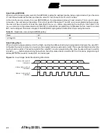
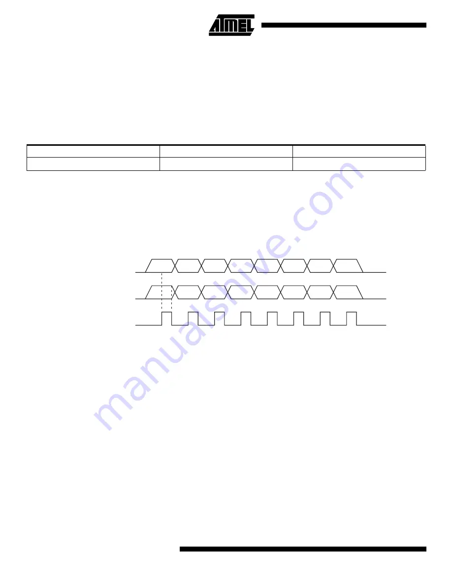
Figure 34. Low-Voltage Serial Downloading Waveforms
Table 16. Read back value during EEPROM polling
Part
P1
P2
ATtiny22/L
$00
$FF
MSB
MSB
LSB
LSB
SERIAL CLOCK INPUT
PB2(SCK)
SERIAL DATA INPUT
PB0(MOSI)
SERIAL DATA OUTPUT
PB1(MISO)

