6
Atmel AVR1923
8394B-AVR-02/12
4 Connectors
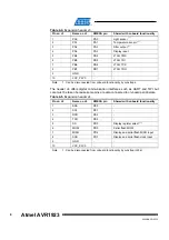
The Atmel AVR XMEGA-A3BU Xplained kit has five 10-pins, 100mil headers. One
header is used for programming the Atmel AVR ATxmega256A3BU, and the others
are used to access spare analog and digital pins on the Atmel AVR XMEGA
(expansion headers).
4.1 Programming headers
The XMEGA can be programmed and debugged by connecting an external
programming/debugging tool to the “JTAG & PDI” header shown in
header has a standard pin-out and therefore tools like the Atmel JTAGICE 3 or Atmel
AVR ONE! can be connected to the header.
Due to physical differences of the Atmel AVR JTAGICE mkII and AVR ONE! probes,
the PCB has an opening below the JTAG and PDI header. This is to make room for
the orientation tap on the JTAGICE mkII probe.
The grey female 10-pin header on JTAGICE mkII has to be used when connecting to
the kit. The opening in the board is made to fit the orientation tab on the header.
When using PDI with the JTAGICE mkII it is necessary to use the squid cable.
A standoff adapter (no. 1) is needed when using AVR ONE!
Pin 1 on the JTAG header is at the top right corner and is marked with a square pad.
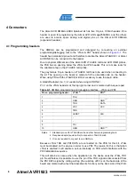
Table 4-1.
XMEGA programming and debugging interface – JTAG and PDI.
Pin on programming header
JTAG
(
PDI
)
1 TCK
-
(
3 TDO
DATA
4 VCC
VCC
5 TMS
-
6 nSRST
CLK
7 -
-
8 -
-
9 TDI
-
(
Notes: 1. Standard pin-out for JTAGICE mkII and other Atmel programming tools.
2. Requires adapter (squid cable) to connect a JTAGICE mkII.
3. It is only required to connect to one GND pin.
Because JTAG TDO and PDI DATA are connected on the PCB for this kit, JTAG
must be disabled on the device in order to use PDI. The reason for this is that when
JTAG is enabled it will enable a pull-up internally on TDO which interferes with the
PDI initialization sequence.
This will also be an issue when the application on the device uses the JTAG_TDO
pin. Nevertheless it is possible to use the pin if the TDO signal is disconnected from
the PDI DATA signal by cutting a strap (the cut-strap J203 is on the back side of the
board and marked with a text that describes its function) on the back side of the PCB.

