AVR180
6
Alternative 2: Low-Cost
Characteristics
•
Low-Component Count
•
Very Low-Cost
•
Small Footprint
•
Short Response Time
•
Small Hysteresis
•
Output Drops Slowly with V
CC
•
Low Accuracy (
±
4-8%)
•
High Current Consumption
•
Sensitive to Component Variations
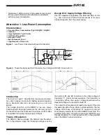
Figure 3a. Low-Cost Brown-Out Detector
Figure 3b. Low-Cost Brown-Out Detector with Manual
Reset Button
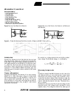
Figure 4. These Oscilloscope Plots Show how the Voltage on RESET Varies with V
CC
Introduction
Figure 3a is showing a circuit that features low cost and
small physical size. However, its high current consumption
might make it unsuited for battery operated applications. As
the voltage transition on the RESET pin is fairly slow when
V
CC
drops, the circuit is sensitive to inaccuracies in compo-
nent values. Due to inaccuracies in resistors R1 and R2,
transistor T1 and AVR MCU RESET threshold value, the
threshold value V
T
should be chosen minimum 15% below
nominal V
CC
.
Theory of Operation
During normal operation, the transistor T1 is open, keeping
RESET at V
CC
. When the supply voltage V
CC
drops below
the threshold voltage (V
T
), the transistor T1 closes. This
allows resistor R3 to pull RESET low (active). The closing
of the transistor T1 occurs when the voltage from emitter to
base drops below a certain value, usually 0.7 volts in small
signal silicon transistors.
R1 and R2 is a voltage divider that controls the emitter-
base voltage. The threshold voltage, V
T
, is defined by:
Choosing Components
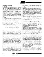
T1
Almost any small signal PNP transistor can be used. One
with high gain (
β
/h
FE
) is recommended as it gives faster
transitions in the output voltage with variations in VCC
around the threshold voltage. Faster transitions make the
circuit more immune to component variation, reducing the
need to calibrate the detector. Also see “Threshold Accu-
racy” on page 4.
Calibration is also required if the threshold voltage for the
transistor varies. This voltage is the constant 0.7 in the
equation above. The voltage is stable for the same type of
AVR
V
CC
R2
R1
RESET
GND
T1
R3
V
CC
100 - 50K
AVR
V
CC
R2
R1
GND
T1
R3
RESET
100 - 50K
V
CC
ISP
R4
OPTIONAL
RESET
SWITCH
V
T
0.7
R1
R2
+
R2
---------------------
or
R1
R2
-------
V
T
0.7
--------
1
–
≈
,
⋅
≈
Summary of Contents for AVR180
Page 10: ...AVR180 10...
Page 11: ...AVR180 11...


