background image

APC-2132 

2    APC-2132 Quick Reference Guide


FCC Statement


THIS  DEVICE  COMPLIES  WITH  PART  15  FCC  RULES.  OPERATION  IS 

SUBJECT TO THE FOLLOWING TWO CONDITIONS: 

(1) THIS DEVICE MAY NOT CAUSE HARMFUL INTERFERENCE. 

(2)  THIS  DEVICE  MUST  ACCEPT  ANY  INTERFERENCE  RECEIVED  INCLUDING 

INTERFERENCE THAT MAY CAUSE UNDESIRED OPERATION. 

THIS  EQUIPMENT  HAS  BEEN TESTED AND  FOUND  TO  COMPLY WITH THE  LIMITS 

FOR A CLASS "A" DIGITAL DEVICE, PURSUANT TO PART 15 OF THE FCC RULES. 

THESE LIMITS ARE DESIGNED TO PROVIDE REASONABLE PROTECTION AGAINST 

HARMFUL  INTERFERENCE  WHEN  THE  EQUIPMENT  IS  OPERATED  IN  A 

COMMERCIAL  ENVIRONMENT.  THIS  EQUIPMENT  GENERATES,  USES,  AND  CAN 

RADIATE  RADIO  FREQUENCY  ENERGY  AND,  IF  NOT  INSTATLLED  AND  USED  IN 

ACCORDANCE  WITH  THE  INSTRUCTION  MANUAL,  MAY  CAUSE  HARMFUL 

INTERFERENCE TO RADIO COMMUNICATIONS. 

OPERATION  OF  THIS  EQUIPMENT  IN  A  RESIDENTIAL  AREA  IS  LIKELY  TO  CAUSE 

HARMFUL  INTERFERENCE  IN  WHICH  CASE  THE  USER  WILL  BE  REQUIRED  TO 

CORRECT THE INTERFERENCE AT HIS OWN EXPENSE. 


A Message to the Customer 

 
Avalue Customer Services 

Each  and  every  Avalue’s  product  is  built  to  the  most  exacting  specifications  to  ensure 

reliable  performance  in  the  harsh  and  demanding  conditions  typical  of  industrial 

environments. Whether your new Avalue device is destined for the laboratory or the factory 

floor, you can be assured that your product will provide the reliability and ease of operation 

for which the name Avalue has come to be known. 
Your satisfaction is our primary concern. Here is a guide to Avalue’s customer services. To 

ensure you get the full benefit of our services, please follow the instructions below carefully. 

 
Technical Support 

We  want  you  to  get  the  maximum  performance  from  your  products.  So  if  you  run  into 

technical difficulties, we are here to help. For the most frequently asked questions, you can 

easily find answers in your product documentation. These answers are normally a lot more 
detailed than the ones we can give over the phone. So please consult the user’s manual 

first. 


To receive the late

st version of the user’s manual; please visit our Web site at: 

http://www.avalue.com.tw/


Summary of Contents for APC-2132

Page 1: ... APC 2132 21 5 6th Gen Intel Core i7 i5 i3 Celeron Expantable Ultra light Multi Touch Fanless Panel PC Quick Reference Guide 2nd Ed 31 October 2017 Copyright Notice Copyright 2017 Avalue Technology Inc ALL RIGHTS RESERVED ...

Page 2: ...TERFERENCE AT HIS OWN EXPENSE A Message to the Customer Avalue Customer Services Each and every Avalue s product is built to the most exacting specifications to ensure reliable performance in the harsh and demanding conditions typical of industrial environments Whether your new Avalue device is destined for the laboratory or the factory floor you can be assured that your product will provide the r...

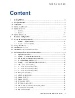
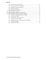
Page 3: ...tings 18 2 5 1 Clear CMOS JCOMS1 18 2 5 2 Serial port 1 2 pin9 signal select JRI1 JRI2 18 2 5 3 LCD backlight brightness adjustment JBKLSEL1 19 2 5 4 AT ATX auto power on select JAT1 19 2 5 5 Serial port 1 in RS 232 422 485 mode JCOM1_SEL1 20 2 5 6 LCD Inverter connector JBKL1 20 2 5 7 On board header for USB2 0 JUSB1 21 2 5 8 On board header for USB2 0 JUSB2 21 2 5 9 On board header for USB2 0 JU...

Page 4: ...r COM1 30 2 6 ARC SKLU DB B Overviews 31 2 7 ARC SKLU DB B Jumper and Connector list 32 2 8 ARC SKLU DB B Jumpers Connectors settings 33 2 8 1 Serial port 1 in RS 232 422 485 mode JCOMSEL1 33 2 8 2 Audio connector JMIC1 33 2 8 2 1 Signal Description Audio connector JMIC1 33 2 8 3 Serial port 1 connector JCOM1 34 2 8 4 RS 422 RS 485 Termination Resistance connector JCOMS1 34 2 8 5 B2B connector B2B...

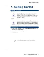
Page 5: ...ics personnel should open the PC chassis Caution Always ground yourself to remove any static charge before touching the CPU card Modern electronic devices are very sensitive to static electric charges As a safety precaution use a grounding wrist strap at all times Place all electronic components in a static dissipative surface or static shielded bag when they are not in the chassis 1 2 Packing Lis...

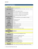
Page 6: ...DC adapter 19V 3 78A BCC ADP 072N 01R Speaker 0 5W 2 Camera By optional Wireless LAN By optional mini PCIe module Bluetooth By optional mini PCIe module Operating System Support Win 7 8 10 Linux Expansion Card 1 full size mini PCIe slot 1 half size mini PCIe slot by IET module Storage Hard Disk Drive By SATA port Solid State Drive By SATA port Panel LCD Panel 21 5 AUO T215HVN01 E96892X5022R 15 2W ...

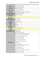
Page 7: ...nsion 539 6 x 342 6 x 45 5mm Weight 6 2kg Color Black plastic Fanless Yes OS Support Windows 7 8 10 Linux Reliability EMI Test CE FCC class B Dust and Rain Test Front Panel IP65 Vibration Test Ramdom Vibration Operation Reference IEC60068 2 64 Testing procedures Test Fh Vibration boardband random Test 1 Test PSD 0 00454G Hz 1 5 Grms 2 Test frequency 5 500 Hz 3 Test axis X Y and Z axis 4 Test time ...

Page 8: ...s 4 Test time 30 minutes each axis 5 Test curve Mechanical Shock Test With CF SSD 10Grms IEC 60068 2 27 Half Sine 11ms Drop Test Package drop test Reference ISTA 2A Method IEC 60068 2 32 Test Ed Test Ea Drop Test 1 Test phase One corner three edges six faces 2 Test high 3 Package weight 4 Test drawing Operating Temperature 0 40 degree Operating Humidity 0 90 Relative Humidity Non condensing Storag...

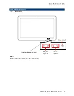
Page 9: ...e Guide APC 2132 Quick Reference Guide 9 1 4 System Overview 1 4 1 Front View Note1 Continue press 4 sec to disable and enable touch function Power on off Brightness Up down Volume Up down Touch enable disable Note1 ...

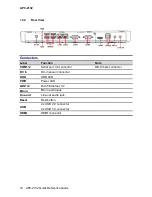
Page 10: ...tion Note COM1 2 Serial port 1 2 connector DB 9 male connector DC in DC in power connector HDD HDD LED PWR Power LED LAN1 2 RJ 45 Ethernet 1 2 Mic in Mic in audio jack Line out Line out audio jack Reset Rest button USB 2 x USB 2 0 connector 4 x USB 3 0 connector HDMI HDMI connector ...

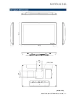
Page 11: ...Quick Reference Guide APC 2132 Quick Reference Guide 11 1 5 System Dimensions Unit mm ...

Page 12: ...Quick Reference Guide 2 Hardware Configuration For advanced information please refer to 1 ARC SKLU and ARC SKLU DB B included in this manual Note If you need more information please visit our website http www avalue com tw ...

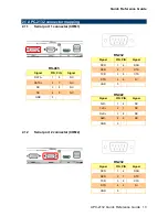
Page 13: ...N PIN Signal DATA 1 6 NC DATA 2 7 NC NC 3 8 NC NC 4 9 NC GND 5 RS 232 Signal PIN PIN Signal DCD 1 6 DSR RXD 2 7 RTS TXD 3 8 CTS DTR 4 9 RI GND 5 RS 422 Signal PIN PIN Signal TxD 1 6 NC TxD 2 7 NC RxD 3 8 NC RxD 4 9 NC GND 5 2 1 2 Serial port 2 connector COM2 RS 232 Signal PIN PIN Signal DCD 1 6 DSR RXD 2 7 RTS TXD 3 8 CTS DTR 4 9 RI GND 5 ...

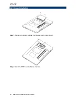
Page 14: ...APC 2132 14 APC 2132 Quick Reference Guide 2 2 Storage Installation Step 1 Remove 2 screws to release the chassis cover and remove it Step 2 Insert the HDD back and fasten 2 screws ...

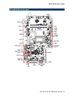
Page 15: ...Quick Reference Guide APC 2132 Quick Reference Guide 15 2 3 ARC SKLU Overviews ...

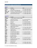
Page 16: ...x 1 wafer pitch 2 00mm JB2B1 B2B connector 40 x 2 wafer pitch 0 80mm JBKLCTL1 LCD backlight brightness adjustment 3 x 2 header pitch 2 00mm LED1 HDD Power LED indicator JLED1 LED connector 3 x 1 header pitch 2 00mm JFP2 Miscellaneous setting connector 5 x 2 wafer pitch 2 00 mm JLVDS1 LVDS connector DIN 40 pin wafer pitch 1 25mm USB1 2 USB connector 1 2 JUSB1 On board header for USB2 0 5 x 1 wafer ...

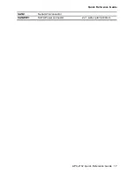
Page 17: ...Quick Reference Guide APC 2132 Quick Reference Guide 17 SATA1 Serial ATA connector SATAPW1 SATA Power connector 2 x 1 wafer pitch 2 00mm ...

Page 18: ...2 18 APC 2132 Quick Reference Guide 2 5 ARC SKLU Jumpers Connectors settings 2 5 1 Clear CMOS JCOMS1 Default Protect Clear CMOS 2 5 2 Serial port 1 2 pin9 signal select JRI1 JRI2 Default Ring 5V 12V JRI1 JRI2 ...

Page 19: ...ference Guide APC 2132 Quick Reference Guide 19 2 5 3 LCD backlight brightness adjustment JBKLSEL1 Default PWM Mode DC Mode 2 5 4 AT ATX auto power on select JAT1 Default Power on by power button Auto power on ...

Page 20: ...5 PIN Signal PIN Signal PIN Signal 12 422RX1 11 COM1 4 10 NDTRA 9 485_422TX1 8 COM1 2 7 NRXDA 6 422RX1 5 COM1 3 4 NTXDA 3 485_422TX1 2 COM1 1 1 NDCDA Note This connector is available after modify the mode of COM1 in BIOS setting 2 5 6 LCD Inverter connector JBKL1 Signal PIN 5V 5 LVDS_BKLT_CTL 4 LVDS_BKLT_EN 3 GND 2 12V 1 ...

Page 21: ...2 Quick Reference Guide 21 2 5 7 On board header for USB2 0 JUSB1 Signal PIN 5VSB 1 USB 2 USB 3 GND 4 GND 5 2 5 8 On board header for USB2 0 JUSB2 Signal PIN PIN Signal 5VSB 2 1 5VSB USB 4 3 USB USB 6 5 USB GND 8 7 GND GND 10 9 GND ...

Page 22: ...APC 2132 22 APC 2132 Quick Reference Guide 2 5 9 On board header for USB2 0 JUSB3 Signal PIN 5VSB 1 USB 2 USB 3 GND 4 GND 5 2 5 10 Battery connector JBAT1 Signal PIN RTCBAT 1 GND 2 ...

Page 23: ..._DATA1_P LVDS_DATA0_N 12 11 LVDS_DATA1_N GND 14 13 GND LVDS_DATA2_P 16 15 LVDS_DATA3_P LVDS_DATA2_N 18 17 LVDS_DATA3_N GND 20 19 GND LVDS_DATA4_P 22 21 LVDS_DATA5_P LVDS_DATA4_N 24 23 LVDS_DATA5_N GND 26 25 GND LVDS_DATA6_P 28 27 LVDS_DATA7_P LVDS_DATA6_N 30 29 LVDS_DATA7_N GND 32 31 GND LVDS_CLK1_P 34 33 LVDS_CLK2_P LVDS_CLK1_N 36 35 LVDS_CLK2_N GND 38 37 GND 12V 40 39 12V ...

Page 24: ...APC 2132 24 APC 2132 Quick Reference Guide 2 5 12 Speaker_R JSPR1 Signal PIN SPK_R 2 SPK_R 1 2 5 13 Speaker_L JSPL1 Signal PIN SPK_L 2 SPK_L 1 ...

Page 25: ...e APC 2132 Quick Reference Guide 25 2 5 14 SPI connector JSPI1 Signal PIN PIN Signal 3 3VSB 1 2 GND SPI0_CS0 3 4 SPI_CLK SPI_SO 5 6 SPI_SI HOLD 7 2 5 15 EC Debug connector JEC1 Signal PIN EC_SMCLK_DEBUG 1 EC_SMDAT_DEBUG 2 ...

Page 26: ...justment JBLK_CTRL1 PIN Signal Note 1 2 BLK_VR_MOD VR must select 10K 1 3 4 BLK_BRI_UP Low pulse button for backlight brighter 5 6 BLK_BRI_DN Low pulse button for backlight dim 2 5 17 UPS GPIO connector JUPS1 Signal PIN PIN Signal OFF_PC 1 2 SMB_CLK GND 3 4 SMB_DATA GND 5 6 GND ...

Page 27: ...K HDMI_HPD 16 56 SMBDATA GND 17 57 GND HDMI1_CTRL_CLK 18 58 BOARD_ID HDMI1_CTRL_DAT 19 59 PCIEUSB3_PONRSTB GND 20 60 PCIEUSB3_SMIB_INT HDMI1_TXN_2 21 61 B2BPCIE_WAKE HDMI1_TXP_2 22 62 RST_B2BPCIE GND 23 63 B2BPCIE_CLK_REQ HDMI1_TXN_1 24 64 GND HDMI1_TXP_1 25 65 PCIE_TXN8 GND 26 66 PCIE_TXP8 HDMI1_TXN_0 27 67 GND HDMI1_TXP_0 28 68 PCIE_RXN8 GND 29 69 PCIE_RXP8 HDMI1_CLKN 30 70 GND HDMI1_CLKP 31 71 ...

Page 28: ...5 19 SATA Power connector SATAPW1 Signal PIN GND 1 5V 2 2 5 20 General purpose I O connector JGPIO1 Signal PIN PIN Signal 3 3V 11 12 GND SMB_DATA 9 10 SMB_CLK DIO_GP23 7 8 DIO_GP13 DIO_GP22 5 6 DIO_GP12 DIO_GP21 3 4 DIO_GP11 DIO_GP20 1 2 DIO_GP10 ...

Page 29: ...Reference Guide 29 2 5 21 Miscellaneous setting connector JFP2 Signal PIN PIN Signal FP_LED1 9 10 FP_LED2 PWRBTN 7 8 LED_ONOFF BRI_DN 5 6 BRI_UP VOL_DN 3 4 VOL_UP GND 1 2 3V 2 5 22 LED connector JLED1 Signal PIN 5VSB 1 LED_BOARD_EN 2 GND 3 ...

Page 30: ...RS 422 and RS 485 changed setting by jumper JCOM_SEL1 RS 232 Signal PIN PIN Signal DCD 1 6 DSR RXD 2 7 RTS TXD 3 8 CTS DTR 4 9 RI GND 5 RS 422 Signal PIN PIN Signal 422_Tx 1 6 NC 422_Tx 2 7 NC 422_Rx 3 8 NC 422_Rx 4 9 NC GND 5 RS 485 Signal PIN PIN Signal 485_Tx 1 6 NC 485_Tx 2 7 NC NC 3 8 NC NC 4 9 NC GND 5 ...

Page 31: ...Quick Reference Guide APC 2132 Quick Reference Guide 31 2 6 ARC SKLU DB B Overviews ...

Page 32: ...nector 5 x 2 header pitch 2 00mm JCOMS1 RS 422 RS 485 Termination Resistance connector 4 x 2 header pitch 2 00mm B2B1 B2B connector 40 x 2 wafer pitch 0 80mm HDMI1 HDMI connector MIC1 Mic in audio jack JMIC1 Audio connector Reserved 6 x 2 wafer pitch 2 00mm LINOUT1 Line out audio jack MINI_PCIE1 Mini PCIe connector USB1 USB connector x 2 JUSB1 USB connector 1 Reserved 5 x 2 wafer pitch 2 00mm JUSB...

Page 33: ... RS422 RS485 2 8 2 Audio connector JMIC1 Signal PIN PIN Signal GND 11 12 MIC_JD LINEIN_JD 9 10 LINEOUT_JD MIC_L 7 8 MIC_R LINE_L_IN 5 6 LINE_R_IN GND 3 4 GND LINE_L_OUT 1 2 LINE_R_OUT 2 8 2 1 Signal Description Audio connector JMIC1 Signal Signal Description LINEOUT_JD AUDIO Out ROUT LOUT sense pin MIC_JD MIC IN MIC_RIN LIN sense pin Note Line in function unavailable ...

Page 34: ... port 1 connector JCOM1 Signal PIN PIN Signal NC 10 9 NRI1 NCTS1 8 7 NRTS1 NDSR1 6 5 GND NDTR1 4 3 NTXD1 NRXD1 2 1 NDCD1 2 8 4 RS 422 RS 485 Termination Resistance connector JCOMS1 Signal PIN PIN Signal GND 8 7 NDTR1 GND 6 5 NDCD1 5V 4 3 NRXD1 5V 2 1 NTXD1 ...

Page 35: ...C 15 55 SMBDATA HDMI_HPD0 16 56 SMBCLK GND 17 57 GND HDMI1_CTRLCLK 18 58 BOARD_ID HDMI1_CTRLDATA 19 59 PONRSTB GND 20 60 NC HDMI1_TXN2 21 61 MPCIE_WAKE HDMI1_TXP2 22 62 MPCIE_RESET GND 23 63 MPCIE_CLKREQ HDMI1_TXN1 24 64 GND HDMI1_TXP1 25 65 MPCIE1_TX GND 26 66 MPCIE1_TX HDMI1_TXN0 27 67 GND HDMI1_TXP0 28 68 MPCIE1_RX GND 29 69 MPCIE1_RX HDMI1_CLK_N 30 70 GND HDMI1_CLK_P 31 71 MPCIE_CLK GND 32 72 ...

Page 36: ...APC 2132 36 APC 2132 Quick Reference Guide 2 8 6 USB connector 2 JUSB2 Signal PIN USBVCC2 1 USB_DN_R_3 2 USB_DP_R_3 3 GND 4 GND 5 ...

Reviews: