background image


AW8155B


            Jul.  2022  V1.3 


www.awinic.com     


3           

COPYRIGHT ©2022 SHANGHAI AWINIC TECHNOLOGY CO. LTD.


Pin Configuration and Top Mark 

INN

CTRL

AGND

AGND

PGND

VOP

VDD

INP

1

2

3

A

B

C

VON

1

2

3

A

B

C

A5
A

XXX

A5A 

 AW8155BFCR

XXX - 

Production Tracing Code

AW8155BFCR MARKING

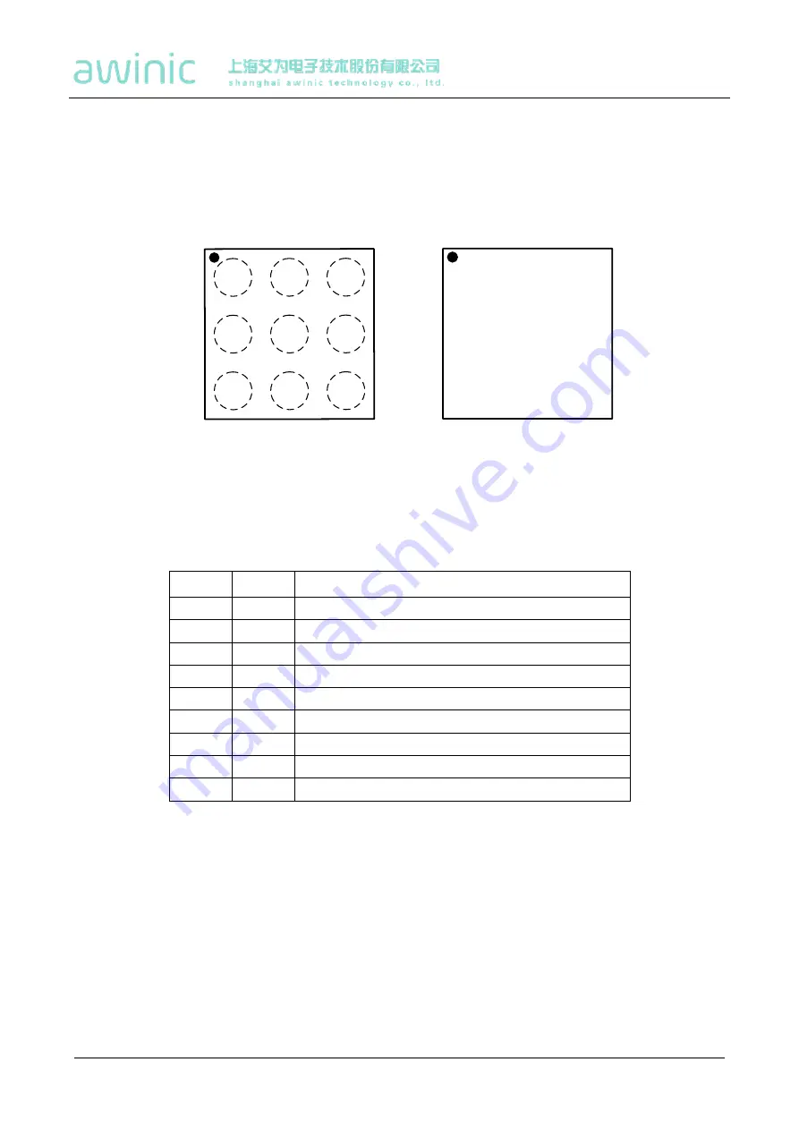
AW8155BFCR TOP VIEW


Figure 2.  

Pin Configuration and Top Mark of AW8155B 

Pin Definition 

No. 

Symbol 

Description 

A1 

INP 

Positive audio input 

A2 

VDD 

Power Supply 

A3 

VOP 

Positive audio output 

B1 

AGND 

Analog ground 

B2 

AGND 

Analog ground 

B3 

PGND 

Power ground 

C1 

INN 

Negative audio input 

C2 

CTRL 

Shutdown and NCN control pin 

C3 

VON 

Negative audio output 


awinic Confidential

Summary of Contents for AW8155B

Page 1: ...hich adjusts the system gain automatically while detecting the Crack distortion of output signal protects the speaker from damage at high power levels and invites the user to bask in immense musical enjoyment AW8155B NCN output power can be set to 0 65w or 0 85w for different speakers this fea ture is embedded in order to protect speakers from damage caused by an excessive sound level The AW8155B ...

Page 2: ...PYRIGHT 2022 SHANGHAI AWINIC TECHNOLOGY CO LTD Typical Application VON INP AGND VDD VOP INN PGND Cs 1μF AW8155B CTRL Cin 33nF Cin 33nF GPIO 10k Figure 1 AW8155B Application Schematic With Single Ended Input a w i n i c C o n f i d e n t i a l ...

Page 3: ...ction Tracing Code AW8155BFCR MARKING AW8155BFCR TOP VIEW Figure 2 Pin Configuration and Top Mark of AW8155B Pin Definition No Symbol Description A1 INP Positive audio input A2 VDD Power Supply A3 VOP Positive audio output B1 AGND Analog ground B2 AGND Analog ground B3 PGND Power ground C1 INN Negative audio input C2 CTRL Shutdown and NCN control pin C3 VON Negative audio output a w i n i c C o n ...

Page 4: ... INP AGND VDD VOP INN PGND Cs 1μF AW8155B CTRL Cin 33nF Cin 33nF GPIO 10k Figure 3 AW8155B Application Schematic With Single Ended Input VON INP AGND VDD VOP INN PGND Cs 1μF AW8155B CTRL Cin 33nF Cin 33nF GPIO 10k Figure 4 AW8155B Application Schematic With Differential Input a w i n i c C o n f i d e n t i a l ...

Page 5: ...Cs 1μF AW8155B CTRL Cin 33nF Cin 33nF GPIO 10k HAC Inductor Figure 5 AW8155B HAC Application Schematic With Single Ended Input VON INP AGND VDD VOP INN PGND Cs 1μF AW8155B CTRL Cin 33nF Cin 33nF GPIO 10k HAC Inductor Figure 6 AW8155B HAC Application Schematic With Differential Input a w i n i c C o n f i d e n t i a l ...

Page 6: ...odel 2kV CDM charged device model 1 5kV Latch Up Test condition JESD78E IT 200mA IT 200mA NOTE1 Conditions out of those ranges listed in absolute maximum ratings may cause permanent damages to the de vice In spite of the limits above functional operation conditions of the device should within the ranges listed in recom mended operating conditions Exposure to absolute maximum rated conditions for p...

Page 7: ...THD N 1 RL 8Ω 33uH VDD 5V 1 30 W THD N 10 RL 4Ω 33uH VDD 4 2V 1 94 W THD N 1 RL 4Ω 33uH VDD 4 2V 1 60 W THD N 10 RL 8Ω 33uH VDD 4 2V 1 13 W THD N 1 RL 8Ω 33uH VDD 4 2V 0 94 W THD N 10 RL 4Ω 33uH VDD 3 6V 1 40 W THD N 1 RL 4Ω 33uH VDD 3 6V 1 14 W THD N 10 RL 8Ω 33uH VDD 3 6V 0 84 W THD N 1 RL 8Ω 33uH VDD 3 6V 0 68 W Mode 1 Iq Quiescent current VDD 3 6V Input AC grounded no load 3 0 mA η Efficiency ...

Page 8: ...utput noise f 20Hz 20kHz input AC grounded 76 uV SNR Signal to noise ratio VDD 5 V PO 1 W RL 8Ω 33uH 93 dB Mode 4 Iq Quiescent current VDD 3 6V Input AC grounded no load 3 5 mA η Efficiency VDD 3 6V Po 0 8W RL 8Ω 33uH 78 Av Voltage gain 11 12 13 V V PSRR Power suppression ratio VDD 4 2V Vp p_sin 200mV 217Hz 70 dB 1kHz 68 dB THD N Total harmonic distortion plus noise VDD 4 2V Po 0 5W RL 8Ω 33uH 0 2...

Page 9: ...st setup Low pass filter uses resistance and capacitor values listed in Table 1 Table 1 AW8155B recommended values for low pass filter Rfilter Cfilter Low pass cutoff frequency 500Ω 10nF 32kHz 1kΩ 4 7nF 34kHz Output Power Calculation According to the above test methods the differential analog output signal is obtained at the output of the low pass filter The valid values Vo_rms of the differential...

Page 10: ...AW8155B Jul 2022 V1 3 www awinic com 10 COPYRIGHT 2022 SHANGHAI AWINIC TECHNOLOGY CO LTD Typical Operating Characteristic a w i n i c C o n f i d e n t i a l ...

Page 11: ...CO LTD OUTPUT POWER vs VIN OUTPUT POWER W VIN Vp 0 5 NCN 0 01 0 05 0 1 0 5 1 2 0 2 0 4 1 2 0 1 OUTPUT POWER vs VIN OUTPUT POWER W VIN Vp 0 5 0 01 0 05 0 1 0 5 1 2 0 2 0 4 1 2 0 1 mode1 VDD 4 2V f 1kHz RL 8Ω 33μH NCN mode2 VDD 4 2V f 1kHz RL 8Ω 33μH a w i n i c C o n f i d e n t i a l ...

Page 12: ...SHANGHAI AWINIC TECHNOLOGY CO LTD NCN POWER vs SUPPLY VOLTAGE Supply Voltage V NCN Output Power W 0 00 0 10 0 20 0 30 0 40 0 50 0 60 0 70 0 80 0 90 1 00 3 4 3 6 3 8 4 4 2 4 4 4 6 RL 8Ω 33uH f 1kHz mode1 mode2 0 65w 0 85w a w i n i c C o n f i d e n t i a l ...

Page 13: ... Class_D start up time Class_D shutdown time VOP VON 10ms div CTRL VOP VON 50us div CTRL VOP VON 10ms div CTRL VOP VON 50us div CTRL Class_AB start up time Class_AB shutdown time Vin VOP VON 10ms div Vin VOP VON 200ms div NCN release time NCN attack time a w i n i c C o n f i d e n t i a l ...

Page 14: ...TECHNOLOGY CO LTD Functional Block Diagram AW8155B PGND INN Input Buffer INP Class D Modulator EEE Module Output Stage CTRL NCN System Control VDD AGND Oscillator OCP OTP VOP VON Class AB RNS Figure 9 Functional Block Diagram of AW8155B a w i n i c C o n f i d e n t i a l ...

Page 15: ...sign The over current over temperature is pre pared inside of the device The AW8155B is available in an ultra small FCQFN 1 5mmX1 5mm 9L package The AW8155B is specified over the industrial temperature range of 40 to 85 One wire pulse control One wire pulse control technology only needs a single GPIO port to operate the chip complete a variety of functions it is very popular in the area of the GPI...

Page 16: ... are three rising edges internal test mode is enable When there are four rising edges AW8155B start to work in Class AB mode while gain is to be set 21 5dB As shown in figure 12 when CTRL pull down above 1ms AW8155B will enter shutdown mode TH TL 0 75us TL TH 10us Mode 1 Mode 2 Mode 3 Mode 4 TOFF Figure 12 One Wire pulse control When AW8155B work in different mode PIN CTRL should be low above 1ms ...

Page 17: ...WINIC unique circuit architecture Effec tively improve the ability to suppress TDD Noise Conduction noise suppression When the RF power amplifier is operating it will draw the current from the battery by 217Hz frequency Power supply will be introduced to 217Hz power ripple since the battery has a certain internal resistance it will be coupled to the speaker through the audio power amplifier The ab...

Page 18: ...nerable RF radiation effects The reasonable PCB layout can reduce the influence of RF radiation in the design such as shorten the line length of input and output as much as possible audio devices should be shielded and far away from the RF antenna maintain the integrity of the device to audio signal pathway to increase the small bypass capacitor RF signals in the sensitive nodes However in practic...

Page 19: ...of the No Clip function Attack time is set 40ms 55ms in AW8155B Release time Release time is the time it takes for the gain to return to its normal level once the audio signal returns below the NCN threshold A fast release time allows the NCN to react quickly to transients preserving the original dynamics of the audio source However similar to a fast attack time a fast release time contributes to ...

Page 20: ...ches and consume negligible additional power Any power loss associated with the Class D output stage is mostly due to the I2R loss of the MOSFET on resistance and supply current The AW8155B features efficiency of 91 Protection Function When a short circuit occurs between VOP VON pin and VDD GND or VOP and VON the over current circuit shutdown the device preventing the device from being damaged Whe...

Page 21: ...orm a high pass filter with the corner frequency fc Hz 169 RinCin 2 1 fC Setting the high pass filter point high can block the 217Hz GSM noise coupled to inputs Better matching of the input capacitors improves performance of the circuit and also help to suppress pop click noise Cin 33nF Differential Input Cin 33nF INP INN Figure 17 Differential Input Cin 33nF Single Ended Input Cin 33nF INP INN Fi...

Page 22: ...vide a separate short and thick power line to AW8155B the copper width is recommended to be larger than 1 2mm The decoupling capacitors should be placed as close as possible to power supply pin 2 The input capacitors should be close to AW8155B INN and INP input pin the input line should be parallel to suppress noise coupling INP VDD PGND VOP VON CTRL INN AGND AGND Cs 1uF Layer1 Layer2 Layer3 Layer...

Page 23: ...SSIGNMENTS FOR PIN 1 ORIENTATION IN TAPE TAPE DIMENSIONS A0 Dimension designed to accommodate the component width B0 Dimension designed to accommodate the component length K0 Dimension designed to accommodate the component thickness W Overall width of the carrier tape P0 Pitch between successive cavity centers and sprocket hole P1 Pitch between successive cavity centers P2 Pitch between sprocket h...

Page 24: ...SHANGHAI AWINIC TECHNOLOGY CO LTD Package Description 1 50 0 10 1 50 0 10 PIN1 CORNER TOP VIEW SIDE VIEW 0 55 0 05 0 0 05 0 10 REF 8X 0 26 0 05 1 00 REF 0 31 REF BOTTOM VIEW 0 50 TYP 0 50 TYP SYMM SYMM Unit mm C B 3 A 1 2 a w i n i c C o n f i d e n t i a l ...

Page 25: ...Y CO LTD Land Pattern Data 1 00 TYP 0 50 TYP 0 50 TYP C 1 2 3 A B Unit mm METAL SOLDER MASK OPENING 0 05 MAX All AROUND 0 05 MIN All AROUND METAL UNDER SOLDER MASK OPENING SOLDER MASK NON SOLDER MASK DEFINED SOLDER MASK DEFINED 9X 0 26 SYMM SYMM a w i n i c C o n f i d e n t i a l ...

Page 26: ...rate TSmax to Tp 3 second max Preheat temperature TSmin to TSmax 150 to 200 Preheat time ts 60 180 seconds Time above TL 217 tL 60 150 seconds Peak temperature Tp 260 Time within 5 of peak temperature tp 20 40 seconds Ramp down rate 6 second max Time 25 to peak temperature 8 minutes max a w i n i c C o n f i d e n t i a l ...

Page 27: ... Revision History Version Release date Description V1 0 2022 03 30 Initial release V1 1 2022 04 13 Update Typical Operating Characteristic V1 2 2022 06 13 Update POD and Land Pattern Data V1 3 2022 07 29 1 Update Functional Block Diagram 2 Update Reflow a w i n i c C o n f i d e n t i a l ...

Page 28: ...y products in such equipment or applications and therefore such inclusion and or use is at the customer s own risk Applications that are described herein for any of these products are for illustrative purposes only AWINIC Technology makes no representation or warranty that such applications will be suitable for the specified use without further testing or modification All products are sold subject...

Reviews: