background image

SBC8233 All-in-One 386SX CPU Card Series User's Manual 

Watchdog Timer 

((

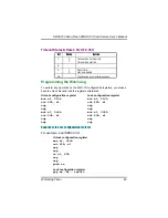
Write data to configuration register 

.> )..;/'#

0!+.+!1"  !

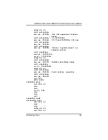
mov al, 03bh 

out 22h, al 

nop 

nop 

mov al, 0ffh 

out 23h, al 

nop 

nop 

+.+!1"  !

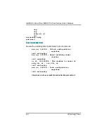
Watchdog Program Example 

 B ? 

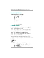
Step 1.   Unlock configuration register. 

Step 2.   Disable watchdog timer by setting INDEX 37H Bit 6 to ‘0’. 

Step 3.   Set the expected counter value to INDEX 3BH, 3AH, 39H. 

Step 4.   Select timeout action from INDEX 38H Bit 7-4. 

Step 5.   Enable watchdog timer by setting INDEX 37H Bit 6 to ‘1’. 

Step 6.   Lock configuration register. 

/> &"1$  -/&/


; Please use MASM to compiler the following program 
; Execute under DOS environment 
dosseg 
. model small 
. stack 100h 
.code 
main proc 

mov ax, 0c513h ; Unlock config. register 
call writechip 
mov ax, 03737h ; Disable watchdog timer 
call readchip 
and al, 10111111b 

Summary of Contents for SBC8233

Page 1: ... ...

Page 2: ... ...

Page 3: ...orporation AMI is a trademark of American Megatrends Inc IBM PC AT PS 2 VGA are trademarks of International Business Machines Corporation Realtek is a trademark of Realtek Semiconductor Corporation All brand names and trademarks are the properties and registered brands of their respective owners ...

Page 4: ... ...

Page 5: ...et Jumper JP1 7 2 3 2 Clear CMOS Setting JP2 7 2 3 3 VGA IRQ9 Operation JP7 7 2 3 4 IRQ3 4 10 11 selection for COM3 COM4 JP9 8 2 3 5 COM2 RS 232 422 485 Setting JP10 8 2 3 6 RS232 422 485 Selection for COM2 Mode JP11 JP12 8 Chapter 3 Chapter 3 Chapter 3 Chapter 3 Hardware Description Hardware Description Hardware Description Hardware Description 3 6 1 Chipset 13 3 6 2 Display Memory 13 3 6 3 VGA F...

Page 6: ... Table of Contents 3 9 2 Serial Ports 5V and 12V Power Selection 17 ...

Page 7: ... Chapter 5 AMI BIOS Setup AMI BIOS Setup AMI BIOS Setup AMI BIOS Setup 6 6 0 7 6 8 8 8 6 0 9 6 Appendix A Appendix A Appendix A Appendix A Watchdog Timer Watchdog Timer Watchdog Timer Watchdog Timer 9 2 9 2 4 8 Chipset Configuration Registers 41 Enable Disable Watchdog INDEX 37H 41 Watchdog Time Out Action INDEX 38H 42 Watchdog Timer INDEX 39H 3AH 3BH 42 Timeout Status Reset INDEX 3CH 43 Programmi...

Page 8: ...gnments System Assignments System Assignments System Assignments 5 Appendix C Appendix C Appendix C Appendix C POST Error Codes POST Error Codes POST Error Codes POST Error Codes 2 2 4 If the Computer Beeps 53 2 Uncompressed Code Checkpoints 56 Runtime Code is Uncompressed 57 ...

Page 9: ......

Page 10: ... ...

Page 11: ...SBC8233 All in One 386SX CPU Card Series User s Manual Introduction 0 1 23 ...

Page 12: ...re defaults bus speeds are programmable up to 16MHz DMA Channels 7 Interrupt Levels 15 Enhanced IDE supports one port and up to two enhanced IDE AT Bus hard drives Watchdog Timer generates a RESET NMI or an IRQ when your application loses control over the system Optionally the watchdog can trigger a user specified interrupt The watchdog is configurable from 30 5μs to 512 seconds in 30 5μs segments...

Page 13: ...FO FDD Interface supports up to two floppy drives 5 360 KB or 1 2 MB and 3 720 KB 1 44 MB Bi directional Parallel Port supports SPP EPP and ECP mode Power Requirements Single voltage 5 V Board Dimensions 185 L x 122 W mm Board Weight 240 g Extended Operating Temperature 0 60 C Chipset TOPRO TP6508IQ Memory 1 MB onboard System Bus 16 bit ISA bus Panel Data Bus 24 bit Display CRT and Flat Panel Mono...

Page 14: ...in One 386SX CPU Card Series User s Manual Introduction 0 Package Single Chip Flash Disk in 32 pin DIP JEDEC Capacity Up to the most updated capacity Data Reliability ECC EDC error correction Memory Window 8 Kbyte ...

Page 15: ...SBC8233 All in One 386SX CPU Card Series User s Manual Installation 4 1 2 0 3 4 ...

Page 16: ...es User s Manual Installation 44 pin Flat Panel Display Parallel Port CONT7 PC 104 Bus 40 pin PC 104 Bus 64 pin IDE FDD Connector GND GND 12V 12V 5V NC External PS 2 AT K B External CRT Display Power Connector JP11 JP12 LED1 Internal K B 2 ...

Page 17: ...r COM3 IRQ10 Short 3 5 JP9 IRQ3 4 10 11 selection for COM4 IRQ11 Short 4 6 JP10 RS 232 422 485 selection for COM2 RS 232 Short 1 2 JP11 RS 232 422 485 for COM2 mode RS 232 Short 3 5 4 6 JP12 RS 232 422 485 for COM2 mode RS 232 Short 3 5 4 6 Options Settings Reset Short 1 2 Normal Open default Options Settings Clear CMOS Short 1 2 Normal Open default Options Settings VGA Operation w o IRQ9 Open def...

Page 18: ...OM3 Short 1 3 Open Short 3 5 default Open COM4 Open Short 2 4 Open Short 4 6 default 0 1 20 COM2 Mode Settings RS 232 Short 1 2 CONT11 active default RS 422 Short 3 4 RS 485 Short 5 6 3 20 4 Options JP11 JP12 RS232 Short 3 5 4 6 default Short 3 5 4 6 default RS 422 485 Short 1 3 2 4 Short 1 3 2 4 ...

Page 19: ... 104 bus 64 pin CONT14 Internal 10 pin box header connector for COM4 CONT3 PC 104 bus 40 pin CONT15 Internal 10 pin box header connector for COM1 CONT4 External PS 2 and AT keyboard JP3 Power LED CONT6 Power JP6 IDE LED CONT7 Internal AT keyboard P1 Parallel Port CONT9 FDD SIM1 Memory bank 0 EDO DRAM COM1 External 9 pin male D type connector for COM1 SIM2 Memory bank 1 EDO DRAM CONT11 Internal 10 ...

Page 20: ...SBC8233 All in One 386SX CPU Card Series User s Manual ...

Page 21: ...SBC8233 All in One 386SX CPU Card Series User s Manual Hardware Description 69 3 6 5 0 21 84 6 0 1 0 36 0 06 0 4 36 0 2 2 51 66 6 6 1 6 14 4 1 6 6 6 6 0 36 ...

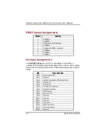
Page 22: ...eyboard IRQ2 Interrupt rerouting from IRQ8 through IRQ15 IRQ3 Serial port 2 IRQ4 Serial port 1 IRQ5 Parallel port 2 IRQ6 Floppy disk controller IRQ7 Parallel port 1 IRQ8 Real time clock IRQ9 Reserved IRQ10 Serial port 3 IRQ11 Serial port 4 IRQ12 PS 2 Mouse IRQ13 Math coprocessor IRQ14 Primary IDE channel IRQ15 Secondary IDE Channel 6 3 0 2 ...

Page 23: ... Data 5 8 Data 10 9 Data 4 10 Data 11 11 Data 3 12 Data 12 13 Data 2 14 Data 13 15 Data 1 16 Data 14 17 Data 0 18 Data 15 19 GND 20 No connector 21 No connector 22 GND 23 IOW 24 GND 25 IOR 26 GND 27 No connector 28 No connector 29 No connector 30 GND Default 31 Interrupt IRQ14 32 IOCS16 33 SA1 34 No connector 35 SA0 36 SA2 37 HDC CS0 38 HDC CSI 39 HDD Active 40 GND 2 CD3 3 0 0 4 E CD3 CD3 6 CD3 6 ...

Page 24: ... HSYNC 7 GND 8 GND 14 VSYNC 9 No connector 10 GND 15 No connector CON2 44 pin Connector for Flat Panel Pin Description Pin Description Pin Description 1 12V 2 12V 3 GND 4 GND 5 VDDM 6 VDDM 7 FPVEE 8 GND 9 PO 10 P1 11 P2 12 P3 13 P4 14 P5 15 P6 16 P7 17 P8 18 P9 19 P10 20 P11 21 P12 22 P13 23 P14 24 P15 25 P16 26 P17 27 P18 28 P19 29 P20 30 P21 31 P22 32 P23 33 GND 34 GND 35 SCLK 36 FLM 37 M 38 LP ...

Page 25: ...valent of HSYNC FLM First line marker Flat panel equivalent of VSYNC 12VM 12V power controlled by chipset ENAVEE Power sequencing controls for panel LCD bias volt VDDM 5V 7 0 2 2 4F 51 6 21 6 CONT9 FDD Connector Pin Assignment Pin No Signal Pin No Signal 1 33 odd GND 20 Step Pulse 2 High Density 22 Write Data 4 6 Unused 24 Write Enable 8 Index 26 Track 0 10 Motor Enable A 28 Write Protect 12 Drive...

Page 26: ...9 IEEE 1284 compliant High speed mode Microsoft and Hewlett Packard extended capabilities port ECP IEEE 1284 compliant 5 G 1 15 G 0 60 Pin Description Pin Description 1 Strobe 2 Data 0 3 Data 1 4 Data 2 5 Data 3 6 Data 4 7 Data 5 8 Data 6 9 Data 7 10 Acknowledge 11 Busy 12 Paper Empty 13 Printer Select 14 Auto Form Feed 15 Error 16 Initialize 17 Printer Select In 18 GND 19 GND 20 GND 21 GND 22 GND...

Page 27: ...2 1C 8 7 60 6 06 H4C2H 1C 7 1 1 CONT11 13 14 15 COM2 3 4 1 Serial Port Connectors Pin Assignment Pin Description Pin Description 1 Data Carrier Detect DCD 2 Data Set Ready DSR 3 Receive Data RXD 4 Request to Send RTS 5 Transmit Data TXD 6 Clear to Send CTS 7 Data Terminal Ready DTR 8 Ring Indicator RI 9 Ground GND 10 Ground GND 112 4 2 061 ...

Page 28: ...of the DiskOnChip is aligned with pin 1 of the socket 3 Set address for both DiskOnChip devices note that the last two settings are for normal EPROM or Flash devices 4 Power up the system 5 During power up you may observe the messages displayed by the DiskOnChip when its drivers are automatically loaded into system s memory 6 At this stage the DiskOnChip can be accessed as any disk in the system 7...

Page 29: ...bootable a Copy the operating system files into the DiskOnChip by using the standard DOS command for example sys d b The DiskOnChip should be the only disk in the systems or should be configured as the first disk in the system c using the DUPDATE utility 0 6 55 6 3 0 2 6 5 60 36 3 60 36 2 3 21 2 3 4 2 CONT7 CONT4 ...

Page 30: ...20 K CONT2 PC 104 Bus Pin Assignment Pin Pin Name Pin Pin Name Pin Pin Name Pin Pin Name 1 IOCHCHK 2 GND 3 SD7 4 RESETDRV 5 SD6 6 5V 7 SD5 8 IRQ9 9 SD4 10 5V 11 SD3 12 DRQ2 13 SD2 14 12V 15 SD1 16 ENDXFR 17 SD0 18 12V 19 IOCHRDY 20 GND 21 AEN 22 SMEMW 23 SA19 24 SMEMR 25 SA18 26 IOW 27 SA17 28 IOR 29 SA16 30 DACK3 31 SA15 32 DRQ3 33 SA14 34 DACK1 35 SA13 36 DRQ1 37 SA12 38 REFRESH 39 SA11 40 SYSCL...

Page 31: ...GND 64 GND CONT3 PC 104 Bus Pin Assignments Pin Pin Name Pin Pin Name Pin Pin Name Pin Pin Name 1 GND 2 GND 3 MEMCS16 4 SBHE 5 IOCS16 6 LA23 7 IRQ10 8 LA22 9 IRQ11 10 LA21 11 IRQ12 12 LA20 13 IRQ15 14 LA19 15 IRQ14 16 LA18 17 DACK0 18 LA17 19 DRQ0 20 MEMR 21 DACK5 22 MEMW 23 DRQ5 24 SD8 25 DACK6 26 SD9 27 DRQ6 28 SD10 29 DACK7 30 SD11 31 DRQ7 32 SD12 33 5V 34 SD13 35 MASTER 36 SD14 37 GND 38 SD15 ...

Page 32: ...User s Manual Hardware Description 11 6 4 CONT6 Power Connector Pin Description Pin Description 1 No connector 4 12V 2 5V 5 GND 3 12V 6 GND JP3 Power LED Pin Description 1 Vcc 2 No connector 3 Ground JP6 IDE LED Pin Description 1 Vcc 2 Signal ...

Page 33: ...019 software compatible Supports PnP auto detect mode 16k byte SRAM built in Supports flash memory read write Supports UTP and auto detect Supports IO address fully decode mode Makes PnP jumper option more user friendly Improves the blinking problem of CRS LED when the cable is not connected ...

Page 34: ...SBC8233 All in One 386SX CPU Card Series User s Manual Ethernet 1 7 1 6 3 6 84 6 3 0 0 ...

Page 35: ...SBC8233 All in One 386SX CPU Card Series User s Manual AMI BIOS Setup 14 0 C 0 0 3 I L M 3 36 0 N 60 L M 60 6 ...

Page 36: ...rement the setting or type the desired value into the field Floppy Drive A B Select the correct specifications for the diskette drive s installed in the computer None No diskette drive installed 360K 5 25 in5 1 4 inch PC type standard drive 1 2M 5 25 in5 1 4 inch AT type high density drive 720K 3 5 in3 1 2 inch double sided drive 1 44M 3 5 in3 1 2 inch double sided drive Hard Disks The BIOS suppor...

Page 37: ... a hard drive the BIOS detects its specifications during POST every time the system boots If you do not want to select drive type AUTO other methods of selecting the drive type are available 1 Match the specifications of your installed IDE hard drive s with the preprogrammed values for drive types 1 through 45 2 Select USER and enter values into each drive parameter field 3 Use the IDE HDD AUTO DE...

Page 38: ...igured BootSector Virus Protection It is not exactly a virus protection All it does is whenever your boot sector is accessed for writing it gives a warning to the screen allowing you to disable the access or to continue Extremely annoying if you use something like OS 2 Boot Manager that needs to write to it It is completely useless for SCSI or ESDI Enhanced Small Device Interface drives as they us...

Page 39: ...other system component System Keyboard Present If Absent is selected this option sets the BIOS to pass the keyboard test in the POST allowing to reset a PC without a keyboard file server printer server etc without the BIOS producing a keyboard error Primary display The type of display standard you are using The most frequent is VGA PGA EGA Modern computers have VGA Video Graphics Array If you have...

Page 40: ...m for both the system as well as the frame buffer memory In other words the size of the DRAM available to the system is reduced by the size of the DRAM allocated to the frame buffer The lower range of the DRAM starting from the DRAM address 00h is allocated to frame buffer The rest of the memory is used by the system ISACLK Set the speed of the ISA bus here The settings are tied to the speed of th...

Page 41: ... configured as 1 MB 15 14MB 2 MB 15 13MB 4 MB 15 11MB 8 MB 15 7MB or disabled 6 Onboard FDC Enable disable or Auto detect FDD Controller Onboard Serial Port1 Disable or enable wtih I O address 3E8h 3F8h as COM1 or 2E8h or 2F8h as COM2 Onboard Serial Port1 Disable or enable wtih I O address 3E8h 3F8h as COM1 or 2E8h or 2F8h as COM2 Onboard Parallel Port This option specifies the parallel port mode ...

Page 42: ... bidirectional data transfer driven by the host device ECP The parallel port can be used with devices that adhere to the Extended Capabilities Port ECP specification ECP uses the DMA protocol to achieve transfer rates of approximately 2 5 Mbs ECP provides symmetric bidirectional communications Parallel Port DMA This option is only available if the setting for the Parallel Port Mode option is ECP T...

Page 43: ...3 0 G 0 63 3 9 3 D 1 3 0 9 0 63 1 9 no Cylinder 1024 x no Head 16 x no Sector 63 x no per sector 512 528 Megabytes G 0 63 G 41 6 P LBA Logical Block Addressing mode 3 G 41 6 9 G G 9 G G 3 D no Cylinder 1024 x no Head 255 x no Sector 63 x bytes per sector 512 814 Gigabytes ...

Page 44: ...U Card Series User s Manual AMI BIOS Setup 1 G 3 G 1 3 3 3 0 G P 3 D CYLS HEADS SECTOR MODE 1120 16 59 NORMAL 560 32 59 LARGE 0 0 0 1 1 3 1 3 G P 6 G no Cylinder 1024 x no Head 32 x no Sector 63 x bytes per sector 512 1 Gigabytes ...

Page 45: ...SBC8233 All in One 386SX CPU Card Series User s Manual AMI BIOS Setup 4 6 4 ENTER PASSWORD L M 60 N L M N L M 7 L M 3 0 PASSWORD DISABLED 0 0 6 0 0 6 ...

Page 46: ...SBC8233 All in One 386SX CPU Card Series User s Manual AMI BIOS Setup 6 7 4 4 ...

Page 47: ...SBC8233 All in One 386SX CPU Card Series User s Manual AMI BIOS Setup 5 6 4 0 4 0 06 ...

Page 48: ...SBC8233 All in One 386SX CPU Card Series User s Manual AMI BIOS Setup 6 8 4 3 QNJ B 60 Q J ...

Page 49: ...SBC8233 All in One 386SX CPU Card Series User s Manual AMI BIOS Setup 8 6 9 3 4 QNJ B Q J ...

Page 50: ...SBC8233 All in One 386SX CPU Card Series User s Manual ...
Page 51: ... 1 4 4 1 4 6 E 1 6 E 4 2 3 E 0 14 E 4 8 E E 4 4 2 6 5 5G G 8G 3G G G 2 Enable Disable Watchdog INDEX 37H Bit Value Action 7 reserved Do not modify the value of these bits 6 0 1 Disable watchdog timer Enable watchdog timer 5 0 Other function Do not modify the value of these bits ...

Page 52: ...000 IRQ11 1001 IRQ12 1010 IRQ14 1011 IRQ15 1100 NMI 1101 System RESET 1110 No output signal 1111 No output signal 3 0 Other function Do not modify the value of these bits Watchdog Timer INDEX 39H 3AH 3BH Index 3BH 3AH 39H Bits D7 D0 D7 D0 D7 D0 counter VSB LSB For example Index 3Bh 3AH 39H Time out 00h 00h 01h 30 56s 00h 00h 02h 616s 00h 01h 00h 7 8 ms 00h 02h 00h 15 6 ms 01h 00h 00h 2 s 02h 00h 0...

Page 53: ...ut has ocurred 6 5 1 0 Reset timer Has no meaning 4 0 Other function do not modify these bits 7 07889 0 1 1 mov al 013h mov al 013h out 22h al out 22h al nop nop nop nop mov al 0c5h mov al 000h out 23h al out 23h al nop nop nop nop Read the value of a configuration register G 0 1 mov al 03ch out 22h al nop nop in al 23h nop nop push ax 1 pop ax AL result ...

Page 54: ...ing INDEX 37H Bit 6 to 0 Step 3 Set the expected counter value to INDEX 3BH 3AH 39H Step 4 Select timeout action from INDEX 38H Bit 7 4 Step 5 Enable watchdog timer by setting INDEX 37H Bit 6 to 1 Step 6 Lock configuration register 1 Please use MASM to compiler the following program Execute under DOS environment dosseg model small stack 100h code main proc mov ax 0c513h Unlock config register call...

Page 55: ...call writechip mov ax 03838h Select system reset as timeout action call readchip and al 00001111b or al 11010000b xchg ah al call writechip mov ax 03737h Enable watchdog timer call readchip or al 01000000b xchg ah al call writechip mov ax 00013h Lock config register call writechip mov ax 04c00h int 21h main endp readchip proc out 22h al nop nop in al 23h nop nop ret readchip endp writechip proc ou...

Page 56: ...writechip endp end main Reset watchdog timer mov ax 0c513h Unlock configuration register call writechip mov ax 03C3Ch Reset watchdog timer counter call readchip or al 00100000b The counter is reset at xchg ah al out 23h al call writechip mov ax 00013h Lock configuration register call writechip ...

Page 57: ... Interrupt controller 2 0C0 0DF DMA controller 2 0F0 Clear math co processor busy signal 0F1 Reset math co processor 0F8 0FF Math processor 10C 10E RAM ROM disk program port address 120 123 Watch dog timer operation 1F0 1F8 Fixed disk controller 200 207 Game port 300 31F Prototype card 360 36F Reserved 378 37F Parallel port 1 3F0 3F7 Floppy disk controller 3F8 3FF Serial port 1 COM1 2F8 2FF Serial...

Page 58: ...Q0 System timer output IRQ1 Keyboard IRQ2 Interrupt rerouting from IRQ8 through IRQ15 IRQ3 Serial port 2 IRQ4 Serial port 1 IRQ5 Selectable for Parallel port IRQ6 Floppy disk controller IRQ7 Parallel port 1 IRQ8 Real time clock IRQ9 Reserved IRQ10 Reserved IRQ11 Reserved IRQ12 PS 2 mouse IRQ13 Math co processor IRQ14 Primary IDE channel IRQ15 Reserved ...

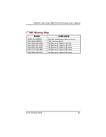
Page 59: ...6SX CPU Card Series User s Manual System Assignments 8 1 2 Address Size Description 00000000h 0009FFFFh 000A0000h 000BFFFFh 000C0000h 000C3FFFh 000C4000h 000C7FFFh 000C8000h 000CBFFFh 000CC000h 000CFFFFh 000D0000h 000DFFFFh ...

Page 60: ...SBC8233 All in One 386SX CPU Card Series User s Manual 4 ...

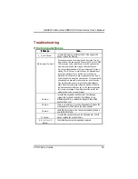
Page 61: ...thin the first 64k of memory 4 System Timer Failure Timer 1 on the system board has failed to function properly 5 Processor Error The CPU on the system board has generated an error 6 Keyboard Controller 8042 Gate A20 error The keyboard controller 8042 contains the gate A20 switch that allows the computer to operate in virtual mode This error message means that the BIOS is not able to switch the CP...

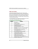
Page 62: ...nable Cache The cache memory test failed Cache memory is disabled Do not press Ctrl Alt Shift to enable cache memory 1 2 short beeps POST failed This is caused by a failure of one of the hardware testing procedures 1 long 2 short beeps Video failure This is caused by one of two possible hardware faults 1 Video BIOS ROM failure checksum error encountered 2 The video adapter installed has a horizont...

Page 63: ... video adapter The system should at least power up and wait for a drive time out Insert the cards back into the system one at a time until the problem happens again When the system does nothing the problem will be with the last expansion card that was put in If the above suggestions fail to cause any change in the malfunction of the system the motherboard must be returned for repair 6 times re ins...

Page 64: ...alue is generated for error checking The previous value is different from the current value CMOS System Options Not Set The values stored in CMOS RAM are either corrupt or nonexistent CMOS Display Type Mismatch The video type in CMOS RAM is not the one detected by the BIOS CMOS Memory Size Mismatch The physical amount of memory on the motherboard is different than the amount in CMOS RAM CMOS Time ...

Page 65: ...rror Interrupt channel 1 failed POST INTR number 2 Error Interrupt channel 2 failed POST Keyboard Error There is a timing problem with the keyboard KB Interface Error There is an error in the keyboard connector Parity Error Parity error is in system memory at an unknown address Memory Parity Error at xxxxx Memory failed at the xxxxx address I O Card Parity Error at xxxxx An expansion card failed a...

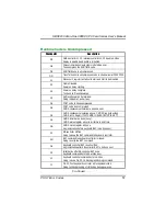
Page 66: ...culation is done CMOS Diag byte written CMOS status register about to init for date and time CB CMOS status register init done Any initialization before keyboard BAT to be done next CD BAT command to keyboard controller is to be issued CE Keyboard controller BAT result verified Any initialization after KB controller BAT to be done next CF Initialization after KB controller BAT done Keyboard comman...

Page 67: ...ecksum calculation to be done next 09 CMOS checksum calculation is done CMOS Diag byte written CMOS init to begin If INIT CMOS IN EVERY BOOT IS SET 0A CMOS initialization done if any CMOS status register about to init for Date and Time 0B CMOS status register init done Any initialization before keyboard BAT to be done next 0C KB controller I B free Going to issue the BAT command to keyboard contro...

Page 68: ...ation about to begin 25 Interrupt Vector initialization done Going to read input port of 9042 for turbo switch if any and to clear password if post diag switch is on 26 Input port of 8042 is read Going to initialize global data for turbo switch 27 Global data initialization for turbo switch is over Any initialization before setting Video mode to be done next 28 Initialization before setting Video ...

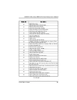
Page 69: ...ferent BUSes 3A New cursor position read and saved Going to display the Hit DEL message 3B Hit DEL message displayed Virtual mode memory test about to start 40 Going to prepare the descriptor tables 42 Descriptor tables prepared Going to enter in virtual mode for memory test 43 Entered in the Virtual mode Going to enable interrupts for diagnostics mode 44 Interrupts enabled if diagnostics switch i...

Page 70: ...t above 1M to follow 52 Memory testing initialization above 1M complete Going to save memory size information 53 Memory size information is saved CPU registers are saved Going to enter in real mode 54 Shutdown successful CPU in real mode Going to disable gate A20 line 57 A20 address line disable successful Going to adjust memory size depending on relocation shadow 58 Memory size adjusted for reloc...

Page 71: ...s cleared About to do programming after setup 89 Programming after setup complete Going to display power on screen message 8B First screen message display WAIT message displayed About to do Main and Video BIOS shadow 8C Main and Video BIOS shadow successful Setup options programming after CMOS setup about to start 8D Set up options are programmed mouse check and init to be done next 8E Mouse check...

Page 72: ...d check is done ID flag set num lock on off keyboard ID command to be issued A0 Keyboard ID command issued Keyboard ID flag to be reset A1 Keyboard ID flag reset Cache memory test to follow A2 Cache memory test over Going to set the keyboard typematic rate A3 Soft error display complete Going to set the keyboard typematic rate A4 Keyboard typematic rate set Going to program memory wait states A5 M...

Page 73: ...ory or Timer 1 on the motherboard is not functioning 5 beeps Processor Error The CPU Central Processing Unit on the motherboard generated an error 6 beeps 8042 Bate A20 Failure Gate A20 on the keyboard controller 8042 allows the CPU to operate in protected mode The BIOS is not able to switch the CPU to protected mode 7 beeps Processor Exception Interrupt Error The CPU generated an exception interr...

Page 74: ...SBC8233 All in One 386SX CPU Card Series User s Manual ...
Reviews: