background image

- 10 -

6.   Power Amplification and Protection Circuit

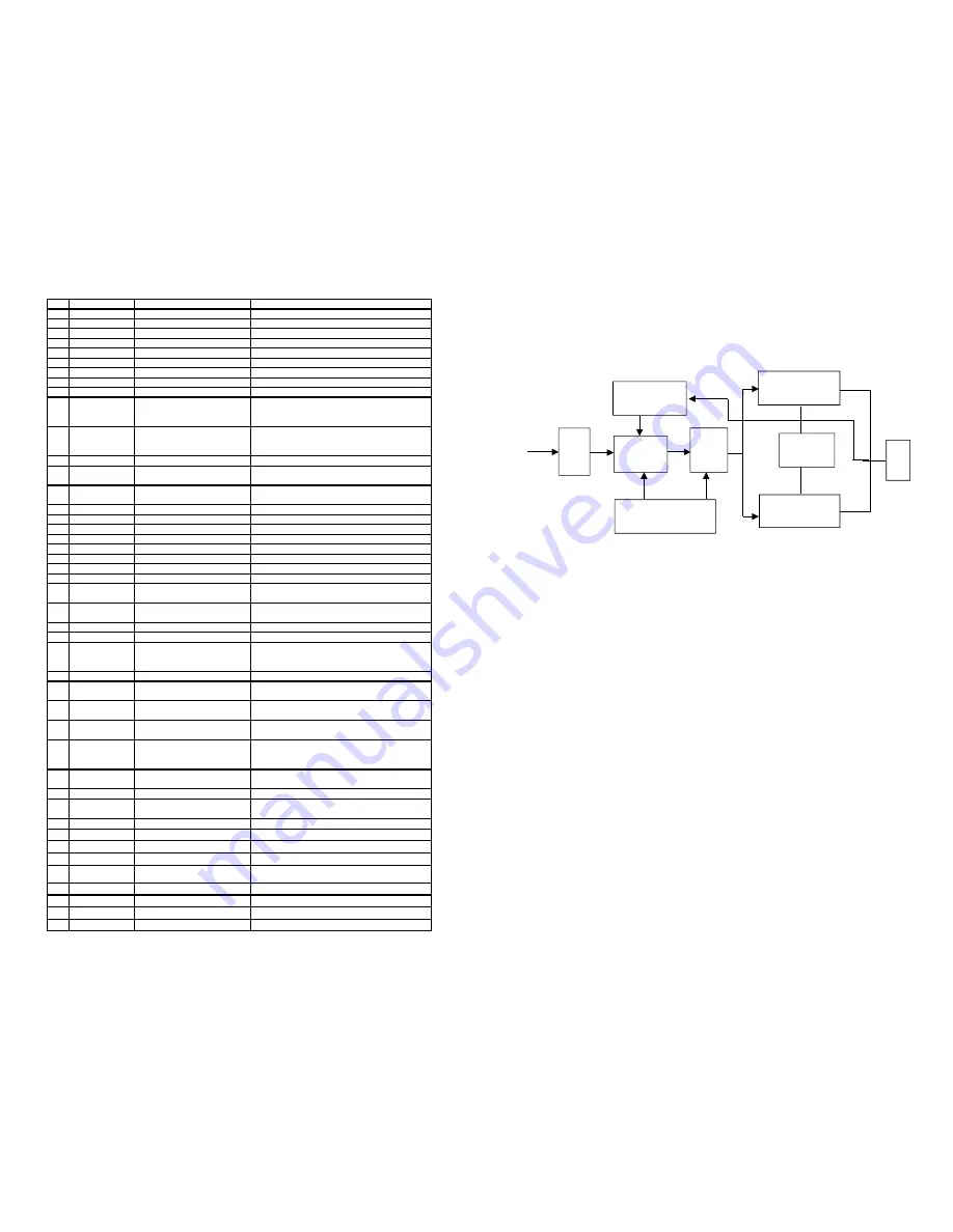
6.1.   Channels L&R Power Amplification Circuit: The L&R power amplifier employs 
separate components. Taking the L channel as an example, its construction is shown 
in Figure 7. 


Differential 

AMP Section


V401,V402


Voltage

AMP

Section


V404


Mirror Image 

Constant Source


V403,V406,VD401,VD402


L Input


Temperature 

Compensation 

Section


V405


Compound 

Power AMP ( PNP)


V409,V410,V412


Compound 

Power AMP ( NPN)


V407,V408,V411


Speakers


AC Negative 

Feedback


R419,R410,C407


(Figure 7)


V440


V441

Mute


The L channel signal is sent to the power amplification section by the electronic volume 
adjusting circuit. A mute circuit installed in the input end. When press the MUTE button 
on the remote control, a high level mute command is sent from the pin 1 of the electronic 
volume adjusting IC N402. It makes V440 and V441 conductive to finish the mute control 
function.

The L channel signal is coupled by the R403&C405 and sent to the base of the differential 
AMP section V401. V401 and V402 compose the single-end input/output differential 
amplification circuit. The audio signal is sent from the collector of V401 to the base of the 
voltage amplification section V404 where its voltage is amplified and sent to the 
compound power amplification section. V403, V406, VD401 and VD402 compose mirror 
image constant circuit. VD401 and VD402 provide constant base current for V403 and 
V405. V403's emitter resistor defines the current of the differential amplification section. 
V406's emitter resistor defines the current of the voltage amplification section. 

V407, V408 and V411 make up the NPN of compound power amplifier. V407 and V408 are
parallel connected. Their function equals a triode (able to amplify power). Then they mix 
with V411 to constitute NPN compound tube (capable of enhance amplification times). 
V409, V410 and V412 constitute the PNP of the compound amplifier. Its circuit 
construction is the same as NPN.  The temperature compensation section V405 has two 
functions in the circuit: First it is a biasing of the NPN and PNP. Its working status defines 
the static working current of the compound power amplification section. That is to say, 
we can adjust the inductance degree of V405 to define the static working point of the 
compound power amplification section. The usual way is to adjust the base resistor of 
V405. It can also automatically adjust the working status of the compound power 
amplification section when the temperature rises.

6.2   C, SR and SL power amplification circuit: These three channels employ the 
exclusive power amplifier IC LM1875 (or TDA2030). It has five pins and is a good power 
amplifier IC. The application circuit is very simple. It has 15W power output in the rated 
condition. The pins 5 & 3 are the positive/negative power supplying pins and employ 
2

¡À

2

V

.


T

h

e


p

in


1


is


th

e


s

ig

n

a

in

p

u

te

rm

in

a

l. 

T

h

e


p

in


2


is


th

e


fe

e

d

b

a

c

k


in

p

u

te

rm

in

a

l. 

T

h

e


p

in


4


is


th

e


o

u

tp

u

te

rm

in

a

l.

- 17 -

30

CD

CD11 25V220U±20%8×12 3.5

C415,C416

31

CD

CD11 35V470U±20%10×20 5

C423,C424

32

CD

CD11 50V1U±20%5×11 2

C411,C412

33

CD

CD11 50V10U±20%5×11 2

C435,C436,C437,C438,C417

34

CD

CD11 35V47U±20%6×12  2.5

C439,C440,C441,C442

35

CD

CD11 35V100U±20%8×12  3.5

C418

36

CD

LUA 35V6800U±20

£ ¥

30×45 10

C421,C422

37

DIODE

1N4004

VD407,VD408,VD419

38

DIODE

1N4148

VD401~VD406,VD418

39

DIODE

1N5404

VD410~VD413

40

VOLTAGE
REGULATOR
DIODE

12V 1/2W

VD415,VD414,VD409

41

VOLTAGE
REGULATOR
DIODE

6.8V 1/2W

VD417,VD416

42

TRIODE

2N5401

V404,V408,V414,V418,V429,V431,V433

43

TRIODE

2N5551

V401,V402,V403,V405,V407,V411~V413,V415,V417,
V428,V430,V432

44

TRIODE

9014C

V406,V416,V421,V422,V423,V424,V426,V427,V434,V4
35

45

TRIODE

9015C

V425

46

TRIODE

KB688O

V410,V420

TRIODE

KB688Y

V410,V420

47

TRIODE

KD718O

V409,V419

TRIODE

KD718Y

V409,V419

48

IC

CD4052BCN DIP

N401

49

RELAY

JH4237-024-2H DC24V

Y401,Y402

50

PCB

4217

£ -

3

51

TERMINAL
SOCKET

AV6-8.4-3B

XC2

52

TERMINAL
SOCKET

AV4-8.4-3B

XC1

53

SOCKET

3 PIN 2.5mm

XS3,XS4

54

SOCKET

6 PIN 2.5mm

XS5

55

SOCKET FOR
EXTERNAL
CORDS

WP6-1B

XL1

56

POLE SOCKET

WP4-10A

XC3

57

CONNECTION
CORDS

¦ µ

0.6  SHAPED 7.5mm

W29,W32,W35,W36,W39,W48,W54,W58,W13

58

CONNECTION
CORDS

¦ µ

0.6  SHAPED 10mm

W10~W12,W15,W19~W21,W27,W31,W33,W34,
W37,W43,W44,W47,W51,W53,W55

59

CONNECTION
CORDS

¦ µ

0.6  SHAPED 12.5mm

W14,W16,W49,W50,W56

60

CONNECTION
CORDS

¦ µ

0.6  SHAPED 15mm

W5,W7,W17,W18,W22,W23~W26,W28,W30,W45,W46
,
W40,W41,W52

61

CONNECTION
CORDS

¦ µ

0.6  SHAPED 20mm

W38,W42,W57

62

FUSE TUBE

T6.3AL 250V

FL401,FL402

63

LARGE
RADIATOR

204×80×61 AB217

CONNECT TO THE MAIN AMP BOARD

64

FUSE HOLDER

0 FL401,FL402

65

SMALL CHIP

AB207

FIX THE TRIODES V406 AND V416

66

TAPPING SCREW PB 3×12H  COLOR ZINC

2 FOR SMALL CHIP AND LARGE RADIATOR

67

TAPPING SCREW PWT 3×8×8 COLOR ZINC

2 FOR PCB/RADIATOR

68

MACHINE
SCREW

PWM 3×16×8 COLOR ZINC

4 FOR POWER TUBE / LARGE RADIATOR

69

SCREW NUT

M3

POWER TUBE SCREW

70

SCREW SPACER

¦ µ

3×7.2×0.5

POWER TUBE SCREW

71

SPRING SPACER

¦ µ

3

POWER TUBE SCREW

72

MICA SPACER

24×20×0.1

4 FOR POWER TUBE / LARGE RADIATOR

Summary of Contents for AV210

Page 1: ...ENGLISH AV210 SERVICE MANUAL ...

Page 2: ... r o c e s s i n g a n d E Q a d j u s t m e n t c ir c u it s 3 I n p u t s ig n a l s d e t e c t s e a r c h a n d f r e q u e n c y s p e c t r u m s a m p l i n g c ir c u it s 4 C o n t r o l C i r c u it 1 1 3 3 4 8 10 12 12 16 24 24 25 27 CAUTIONS There is high voltage inside this unit Make sure to pull out the plug of this unit before repairing There are many high voltage components insid...

Page 3: ...ified by N407A and N407B At the same time the pin 32 of CPU N422 sends out a high level to the electronic switch N410 s pins 9 10 and 11 SEL control signal C SR and SL signals are sent out from the N410 s pins 14 15 and 4 to IC N402 where separate volumes are adjusted SW signals D SW is sent to the IC N402 s where the volume is adjusted Therefore the 6 channel signals of 5 1 CH input are selected ...

Page 4: ...ent out from the pin 4 is added to the pin 6 of N402 where the electronic volume is adjusted The pins 10 11 SWLL are high level According to the real value table the central channel signal S C sent out from the pin 14 of N411 and the surround channel signal S S sent out from the pin 15 of N411 are added to the pins 12 2 and 5 of N410 The S S is divided into two signalssurround left and surround ri...

Page 5: ...d of N403A SEARCH is connected to the pin 28 of CPU This control signal is the search and detect signal when it is low level it enters the search mode when it is high level it stops searching Its works as follows 3 1 1 When this unit is getting started the A B control signals from the pins 38 39 in the domination of the CPU s inter program are added to the input select circuit to search circularly...

Page 6: ...d to finish the control functions RP901 finishes the master volume adjustment and RP905 finishes multi function adjustment To Encoder Master R621 680K R618 100K R619 1K R626 1K R622 1K R627 5 6K R623 10k R625 2 2K R620 10K 12V 12V R613 10K R608 10K R603 10K R598 10K R593 10K C524 223 C515 272 C518 682 C521 683 C527 154 R596 1K R597 10K R601 1K R602 10K R594 5 6K R599 5 6K R604 5 6K R609 5 6K R614 ...

Page 7: ...421 2N5401 V422 2N5401 V424 A1694 V418 2N5551 V414 2N5551 V423 C4467 V415 2N5551 V416 2N5401 R430 1K C415 10u 16V R431 47K C416 221 R432 2 7K R434 47 R433 2 7K R446 33K R437 1K C417 100U 16V R435 47 R436 620 R438 33K R439 1k R440 200 C418 33 R443 200 VD406 1N4148 V420 2N5551 V419 2N5551 R445 10 R444 10 R450 10 R449 10 R448 100 0 25W R447 100 0 25W R441 4 7K R442 2K C419 104 C413 100U 50V C412 104 ...

Page 8: ...u 16V C491 4 7u 16V C490 4 7u 16V C489 4 7u 16V C486 4 7u 16V C485 4 7u 16V C484 822 C483 153 C482 334 C487 104 TAPE R VCD L CD R VCD R CD L 5 1CH R 5 1CH L TAPE L X0 12 X1 14 X2 15 X3 11 Y0 1 Y1 5 Y2 2 Y3 4 INH 6 A 10 B 9 VEE 7 X 13 Y 3 16 8 N401 CD4052 C464 47u 16V R530 470 VD432 6 8V VD431 6 8V R529 470 C462 47u 16V 12V 12V R531 1k R532 1k REC R REC L C465 10u 16V C466 10u 16V R527 47k R528 47k...

Page 9: ...reaches the pin 12 of CPU after opposite phased by V437 And then CPU processes it and sends it to front panel display IC N901 which will make dynamic spectrum display on the display As a matter of fact every frequency is displayed sequentially However what we see on the display screen is the working process all the spectrums are displayed simultaneously due to every frequency display circulate ver...

Page 10: ...D DIP N403 N408 N420 IC 4558C DIP N403 N408 N420 105 IC L7812CV GOLD SEALED TO 220 N412 IC LM7812 GOLD SEALED TO 220 N412 106 IC CD4051 DIP N416 N419 107 IC CD4053BCN DIP N410 N411 108 IC CD4052BCN DIP N401 109 IC M62446FP SOP N402 110 IC 24C02 DIP N421 111 I C LM1875T T05B N413 N414 N415 112 SOFTWARE PROGRAM CPU CPU AV210 RU 0 N422 113 CRYSTAL OSCILLATOR 12 00MHz 49 U G601 114 RELAY JH1806 012 3H...

Page 11: ...o is e is f ilt e r e d b y t h e s h o r t c ir c u it W h e n t h e m ic r o p h o n e i s in s e r t e d t h e c o n t a c t c h ip i s c u t o f a n d t h e m ic r o p h o n e c ir c u it h a s n o r m a l o u t p u t N905 PT2399 Echo Processing Automatic Search Detect Circuit V902 AMP N404B N405B Mix with the channels L R N904B RP903 RP904 Figure 6 OK ªMUTE 18 59 PORCELAIN CAPACITOR 50V 683 1...

Page 12: ... power amplification section when the temperature rises 6 2 C SR and SL power amplification circuit These three channels employ the exclusive power amplifier IC LM1875 or TDA2030 It has five pins and is a good power amplifier IC The application circuit is very simple It has 15W power output in the rated condition The pins 5 3 are the positive negative power supplying pins and employ 2 À 2 V T h e ...

Page 13: ...8 When there is one output mid point DC voltage which is higher than 3 5V or lower than 3 5V V429 and V428 are conducted Their base voltage will decrease and V430 is conducted At last the relay switches off and the protection circuit is getting started One over voltage sampling resistor is connected to every R478 connected to L channel Above 3 5V Below 3 5V V429 conducted V428 conducted Collector ...

Page 14: ...BON FILM RESISTOR 1 6W3 3K 5 SHAPED 7 5 R948 13 CARBON FILM RESISTOR 1 6W220K 5 SHAPED 7 5 R962 14 CARBON FILM RESISTOR 1 6W30K 5 SHAPED 7 5 R936 R942 15 CARBON FILM RESISTOR 1 6W8 2K 5 SHAPED 7 5 R937 R939 R934 16 CARBON FILM RESISTOR 1 2W100 5 SHAPED 12 5 R915 CARBON FILM RESISTOR 1 6W56K 5 SHAPED 7 5 R908 17 CARBON FILM RESISTOR 1 6W47 5 SHAPED 7 5 R909 18 CARBON FILM RESISTOR 1 6W470K 5 SHAPED...

Page 15: ...5 T2 2P SHIELD WITH L NEEDLE 4 GROUND PINS XP5 59 RAFT CORDS 9P330 2 5 2 PLUG WITH L NEEDLE XP4 60 RAFT CORDS 4P60 2 5 2 PLUG 3P SHIELD WITH L NEEDLE XP6 61 INFRARED SENSOR HS0038B N902 62 SOFT SPONGE SPACER 10 10 10 DOUBLE FACED HARD N902 PCB 63 SOFT SPONGE SPACER 10 10 5 DOUBLE FACED HARD VFD901 PCB SCHEMATIC DIAGRAM OF THE FRONT CONTROL PANEL BOARD SW1 1 SW2 2 SW3 3 SW4 4 DOUT 5 DIN 6 NC 7 CLK ...

Reviews: