background image

- 4 -

- 23 -

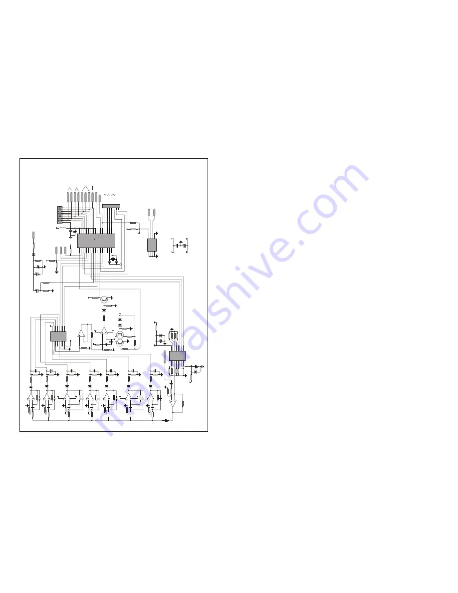
3.2   Spectrum Sampling Amplification Circuit: The routes carrying the five-channel 
signals sent from the IC N402 are connected to the sampling resistors R494, R495, 
R496, R565 and R566 respetively.(The SW channel sends out the signals directly.) After 
being mixed by these resistors, the signals reach N406A to be amplified. The incurred 
spectrum analyzing signal source is sent to the front panel circuit.

4.   Control Circuit.

The control circuit of this player is divided into CPU Circuit, Front Panel Control and 
Display Circuit and Spectrum Analyzing Circuit.

4.1 CPU Circuit

N422 (AT89C540) is this unit's CPU which sends all commands to the command-
controlled circuits to perform all control functions. It incorp5V power supply and 
its pin 40 is the power supply pin. The 12M crystal oscillator provides the work clock for 
itself. The pin 9 is the restoration pin. When this unit is getting started, +5V passes 
VD409 to reach the positive pole of C531. Because of the C531's charging, its negative 
end sends out an instantaneous high level which passes through R686 to reach the pin 
9 of N422. The pin 9 of N422 restores the low level mode with the end of charging. This 
restoration circuit's style is the high level restoration to keep in low level. You can also 
refer to the circuit diagram for other command instructions. 

The static information such as the power-on logo and on screen displays when this unit 
is working is stored in the CPU's static memory. N421 is a power-off-mode memory which 
can record the working information when this unit is turned off and call back these 
information when this unit is turned on next time. Therefore, you need not to readjust the 
unit every time you turn it on. Furthermore, the sound field modes that you set are also 
stored in N421, which can be called back when needed.

4.2  Front panel control and display circuit

This circuit incorporates an exclusive IC N901 (UPD16311). Its pins 10, 11, 12 and 13 
are connected to the press scan matrix which receives the control commands from the 
user and process them into two-line outputs: One line reaches to the VFD to display the 
working modes, another line passes pins 5, 6, 8 and 9 to CPU to finish the control 
functions.

N902 is the remote control sensor. It convert the infrared signals received to electric 
signal and then send it to the pin 13 of CPU to finish the remote control function.

RP901 and RP905 comprise a digital pulse potentiometer. When rotating it, a series of 
digital pulse will be sent out and added to the pins 23, 24, 25 and 26 to be detect and 
processed to finish the control functions. RP901 finishes the master volume adjustment 
and RP905 finishes multi-function adjustment. 

T

o

E

n

c

o

d

e

r

(

M

a

s

te

r

)

R

6

2

1

6

8

0

K

R

6

1

8

1

0

0

K

R

6

1

9

1

K

R

6

2

6

1

K

R

6

2

2

1

K

R

6

2

7

5

.6

K

R

6

2

3

1

0

k

R

6

2

5

2

.2

K

R

6

2

0

1

0

K

+

1

2

V

-1

2

V

R

6

1

3

1

0

K

R

6

0

8

1

0

K

R

6

0

3

1

0

K

R

5

9

8

1

0

K

R

5

9

3

1

0

K

C

5

2

4

2

2

3

C

5

1

5

2

7

2

C

5

1

8

6

8

2

C

5

2

1

6

8

3

C

5

2

7

1

5

4

R

5

9

6

1

K

R

5

9

7

1

0

K

R

6

0

1

1

K

R

6

0

2

1

0

K

R

5

9

4

5

.6

K

R

5

9

9

5

.6

K

R

6

0

4

5

.6

K

R

6

0

9

5

.6

K

R

6

1

4

5

.6

K

R

5

9

5 8

2

K

R

6

0

0 8

2

K

R

6

1

0 8

2

K

R

6

1

5 8

2

K

R

6

0

6

1

K

R

6

0

7

1

0

K

R

6

1

1

1

K

R

6

1

2

1

0

K

R

6

1

6

1

K

R

6

1

7

1

0

K

C

5

1

6

2

7

2

C

5

1

9

6

8

2

C

5

2

5

2

2

3

C

5

2

3

2

.2

U

C

5

2

6

2

.2

U

C

5

2

9

2

.2

u

C

5

2

0

2

.2

U

C

5

1

7

2

.2

U

C

5

2

2

6

8

3

R

6

0

5 8

2

K

1

2

1

3

1

4

N

4

1

7

D

L

M

3

2

4

1

2

1

3

1

4

N

4

1

8

D

L

M

3

2

4

3

2

1

4

11

N

4

1

8

A

L

M

3

2

4

1

0

9

8

N

4

1

7

C

L

M

3

2

4

C

5

2

8

1

5

4

-1

2

V

3

5

H

z

1

0

0

H

z

3

0

0

H

z

1

K

H

z

3

K

H

z

1

0

9

8

N

4

1

8

C

L

M

3

2

4

V

D

4

4

6

1

N

4

1

4

8

V

D

4

4

5

1

N

4

1

4

8

V

D

4

4

4

1

N

4

1

4

8

V

D

4

4

3

1

N

4

1

4

8

V

D

4

4

2

1

N

4

1

4

8

C

5

0

7

1

0

u

/1

6

V

+

1

2

V

R

5

8

8

1

0

K

R

5

8

3

1

0

K

C

5

0

9

1

5

2

C

5

1

2

6

8

1

R

5

8

6

1

K

R

5

8

7

1

0

K

R

5

9

1

1

K

R

5

9

2

1

0

K

R

5

8

4

5

.6

K

R

5

8

9

5

.6

K

R

5

8

5

8

2

K

R

5

9

0

8

2

K

C

5

1

0

1

5

2

C

5

1

3

6

8

1

C

5

1

4

2

.2

U

C

5

1

1

2

.2

U

3

2

1

4

11

N

4

1

7

A

L

M

3

2

4

1

0

K

H

z

1

6

K

H

z

5

6

7

N

4

1

8

B

L

M

3

2

4

V

D

4

4

1

1

N

4

1

4

8

V

D

4

4

0

1

N

4

1

4

8

R

5

8

0

1

K

C

5

0

8

1

0

u

/1

6

V

X

4

1

X

6

2

X

C

O

M

3

X

7

4

X

5

5

IN

H

6

V

E

E

7

V

S

S

8

C

(2

)

9

B

(1

)

1

0

A

(0

)

1

1

X

3

1

2

X

0

1

3

X

1

1

4

X

2

1

5

V

D

D

1

6

N

4

1

6

4

0

5

1

X

4

1

X

6

2

X

C

O

M

3

X

7

4

X

5

5

IN

H

6

V

E

E

7

V

S

S

8

C

(2

)

9

B

(1

)

1

0

A

(0

)

1

1

X

3

1

2

X

0

1

3

X

1

1

4

X

2

1

5

V

D

D

1

6

N

4

1

9

4

0

5

1

R

5

8

1

1

0

K

R

5

8

2

4

7

0

K

5

6

7

N

4

1

7

B

L

M

3

2

4

-1

2

V

+

1

2

V

S

-6

.2

V

3

2

1

8

4

N

4

2

0

A

4

5

5

8

5

6

7

N

4

2

0

B

4

5

5

8

V

D

4

4

7

3

.3

V

+

1

2

V

V

4

3

5

2

N

5

5

5

1

V

4

3

7

2

N

5

5

5

1

E

C

B

V

4

3

6

2

N

5

4

0

1

R

6

2

8

4

.7

K

R

5

7

2 1

8

0

k

R

5

7

1

7

5

k

R

5

7

6

4

.3

k

R

5

7

9 1

0

k

R

5

7

71

.5

k

R

5

7

4

2

7

k

R

5

7

8

2

.2

k

R

6

2

4

1

0

K

V

D

4

4

9

1

N

4

1

4

8

V

D

4

5

0

1

N

4

1

4

8

D

+

5

V

V

D

4

4

8

1

N

4

1

4

8

D

+

5

V

R

5

7

3

4

7

0

k

-1

2

V

+

1

2

V

S

+

6

.8

V

D

IS

1

A

D

IS

1

B

D

IS

1

C

D

IS

2

A

D

IS

2

B

D

IS

2

C

C

5

3

0

1

0

4

1

2

3

4

5

6

7

8

9

1

0

1

1

1

2

1

3

1

4

1

5

1

6

1

7

1

8

1

9

2

0

2

5

4

0

3

9

3

8

3

7

3

6

3

5

3

4

3

3

3

2

3

1

3

0

2

9

2

8

2

7

2

6

2

4

2

3

2

2

2

1

V

c

c

P

0

0

(A

D

0

)

P

0

1

(A

D

1

)

P

0

2

(A

D

2

)

P

0

3

(A

D

3

)

P

0

4

(A

D

4

)

P

0

5

(A

D

5

)

P

0

6

(A

D

6

)

P

0

7

A

D

7

)

E

A

/V

p

p

A

L

E

P

S

E

N

P

2

0

(A

8

)

P

2

1

(A

9

)

P

2

2

(A

1

0

)

P

2

3

(A

1

1

)

P

2

4

(A

1

2

)

P

2

5

(A

1

3

)

P

2

6

(A

1

4

)

P

2

7

(A

1

5

)

P

1

0

(T

2

)

P

1

1

(T

2

)

P

1

2

P

1

3

P

1

4

P

1

5

P

1

6

P

1

7

R

S

T

P

3

0

(R

X

D

)

P

3

1

(T

X

D

)

P

3

2

(I

N

T

0

)

P

3

3

(I

N

T

1

)

P

3

4

(T

0

)

P

3

5

(T

1

)

P

3

6

(W

R

)

P

3

7

(R

D

)

X

T

A

L

2

X

T

A

L

1

G

N

D

N

4

2

2

A

T

8

9

C

5

4

D

IS

P

L

A

Y

1

2

3

4

5

6

7

8

9

X

S

4

8

P

IN

A

S

D

A

L

A

T

C

H

B

S

C

K

C

L

K

D

A

T

A

T

o

 C

D

4

0

5

2

T

o

 M

6

2

4

4

6

R

e

la

y

C

o

n

tr

o

l

R

E

M

O

T

E

C

L

K

D

A

T

A

S

T

B

A

1

B

1

A

2

B

2

T

o

 u

P

D

1

6

3

1

1

T

o

E

n

c

o

d

e

r

1

(

M

a

s

te

r

V

O

L

.)

o

2

J

o

g

C

6

6

1

2

0

P

C

6

6

2

2

0

P

G

4

0

1

1

2

M

L

4

0

6

1

0

0

u

H

D

+

5

V

5

3

4

1

0

4

R

5

7

5

1

k

R

5

7

0

1

k

V

D

4

3

8

6

.8

V

V

D

4

3

9

6

.8

V

C

5

0

6

4

7

u

/1

6

V

C

5

0

5

4

7

u

/1

6

V

S

+

6

.8

V

S

-6

.8

V

1

2

3

4

5

6

7

8

9

R

R

9

0

1

8

*4

.7

K

C

5

3

5

4

7

u

/1

6

V

R

6

2

9

1

0

k

C

5

3

1

1

0

u

/1

6

V

A

0

1

A

1

2

A

2

3

V

S

S

4

S

D

A

5

S

C

L

6

T

E

S

T

7

V

D

D

8

N

4

2

1

2

4

C

0

2

S

C

K

D

+

5

V

S

D

A

S

E

L

S

E

A

R

C

H

T

o

 C

D

4

0

5

3

T

o

 2

4

C

0

2

E

.O

E

K

-M

U

T

R

6

8

7

1

k

R

6

8

8

2

.2

k

V

D

4

0

9

1

N

4

0

0

4

V

D

4

1

0

4

.7

V

C

6

6

5

4

7

u

/1

6

V

P

-R

S

T

S

E

L

1

R

-T

E

X

T

o

 C

D

4

0

5

3

(N

4

1

1

)

R

e

la

y

T

e

s

t(

Y

4

0

2

)

E

x

c

h

a

n

g

e

S

e

a

rc

h

L

e

v

e

l

M

IC

M

u

tt

in

g

R

6

9

0

4

.7

k

R

6

8

9

2

.2

k

+

A

6

V

R

6

8

5

4

.7

k

R

6

9

1

4

.7

k

R

6

8

0

4

.7

k

D

+

5

V

R

6

8

6

1

k

C

6

6

8

4

7

u

/1

6

V

C

6

6

9

4

7

u

/1

6

V

+

1

2

V

+

1

2

V

-1

2

V

-1

2

V

Summary of Contents for AV210

Page 1: ...ENGLISH AV210 SERVICE MANUAL ...

Page 2: ... r o c e s s i n g a n d E Q a d j u s t m e n t c ir c u it s 3 I n p u t s ig n a l s d e t e c t s e a r c h a n d f r e q u e n c y s p e c t r u m s a m p l i n g c ir c u it s 4 C o n t r o l C i r c u it 1 1 3 3 4 8 10 12 12 16 24 24 25 27 CAUTIONS There is high voltage inside this unit Make sure to pull out the plug of this unit before repairing There are many high voltage components insid...

Page 3: ...ified by N407A and N407B At the same time the pin 32 of CPU N422 sends out a high level to the electronic switch N410 s pins 9 10 and 11 SEL control signal C SR and SL signals are sent out from the N410 s pins 14 15 and 4 to IC N402 where separate volumes are adjusted SW signals D SW is sent to the IC N402 s where the volume is adjusted Therefore the 6 channel signals of 5 1 CH input are selected ...

Page 4: ...ent out from the pin 4 is added to the pin 6 of N402 where the electronic volume is adjusted The pins 10 11 SWLL are high level According to the real value table the central channel signal S C sent out from the pin 14 of N411 and the surround channel signal S S sent out from the pin 15 of N411 are added to the pins 12 2 and 5 of N410 The S S is divided into two signalssurround left and surround ri...

Page 5: ...d of N403A SEARCH is connected to the pin 28 of CPU This control signal is the search and detect signal when it is low level it enters the search mode when it is high level it stops searching Its works as follows 3 1 1 When this unit is getting started the A B control signals from the pins 38 39 in the domination of the CPU s inter program are added to the input select circuit to search circularly...

Page 6: ...d to finish the control functions RP901 finishes the master volume adjustment and RP905 finishes multi function adjustment To Encoder Master R621 680K R618 100K R619 1K R626 1K R622 1K R627 5 6K R623 10k R625 2 2K R620 10K 12V 12V R613 10K R608 10K R603 10K R598 10K R593 10K C524 223 C515 272 C518 682 C521 683 C527 154 R596 1K R597 10K R601 1K R602 10K R594 5 6K R599 5 6K R604 5 6K R609 5 6K R614 ...

Page 7: ...421 2N5401 V422 2N5401 V424 A1694 V418 2N5551 V414 2N5551 V423 C4467 V415 2N5551 V416 2N5401 R430 1K C415 10u 16V R431 47K C416 221 R432 2 7K R434 47 R433 2 7K R446 33K R437 1K C417 100U 16V R435 47 R436 620 R438 33K R439 1k R440 200 C418 33 R443 200 VD406 1N4148 V420 2N5551 V419 2N5551 R445 10 R444 10 R450 10 R449 10 R448 100 0 25W R447 100 0 25W R441 4 7K R442 2K C419 104 C413 100U 50V C412 104 ...

Page 8: ...u 16V C491 4 7u 16V C490 4 7u 16V C489 4 7u 16V C486 4 7u 16V C485 4 7u 16V C484 822 C483 153 C482 334 C487 104 TAPE R VCD L CD R VCD R CD L 5 1CH R 5 1CH L TAPE L X0 12 X1 14 X2 15 X3 11 Y0 1 Y1 5 Y2 2 Y3 4 INH 6 A 10 B 9 VEE 7 X 13 Y 3 16 8 N401 CD4052 C464 47u 16V R530 470 VD432 6 8V VD431 6 8V R529 470 C462 47u 16V 12V 12V R531 1k R532 1k REC R REC L C465 10u 16V C466 10u 16V R527 47k R528 47k...

Page 9: ...reaches the pin 12 of CPU after opposite phased by V437 And then CPU processes it and sends it to front panel display IC N901 which will make dynamic spectrum display on the display As a matter of fact every frequency is displayed sequentially However what we see on the display screen is the working process all the spectrums are displayed simultaneously due to every frequency display circulate ver...

Page 10: ...D DIP N403 N408 N420 IC 4558C DIP N403 N408 N420 105 IC L7812CV GOLD SEALED TO 220 N412 IC LM7812 GOLD SEALED TO 220 N412 106 IC CD4051 DIP N416 N419 107 IC CD4053BCN DIP N410 N411 108 IC CD4052BCN DIP N401 109 IC M62446FP SOP N402 110 IC 24C02 DIP N421 111 I C LM1875T T05B N413 N414 N415 112 SOFTWARE PROGRAM CPU CPU AV210 RU 0 N422 113 CRYSTAL OSCILLATOR 12 00MHz 49 U G601 114 RELAY JH1806 012 3H...

Page 11: ...o is e is f ilt e r e d b y t h e s h o r t c ir c u it W h e n t h e m ic r o p h o n e i s in s e r t e d t h e c o n t a c t c h ip i s c u t o f a n d t h e m ic r o p h o n e c ir c u it h a s n o r m a l o u t p u t N905 PT2399 Echo Processing Automatic Search Detect Circuit V902 AMP N404B N405B Mix with the channels L R N904B RP903 RP904 Figure 6 OK ªMUTE 18 59 PORCELAIN CAPACITOR 50V 683 1...

Page 12: ... power amplification section when the temperature rises 6 2 C SR and SL power amplification circuit These three channels employ the exclusive power amplifier IC LM1875 or TDA2030 It has five pins and is a good power amplifier IC The application circuit is very simple It has 15W power output in the rated condition The pins 5 3 are the positive negative power supplying pins and employ 2 À 2 V T h e ...

Page 13: ...8 When there is one output mid point DC voltage which is higher than 3 5V or lower than 3 5V V429 and V428 are conducted Their base voltage will decrease and V430 is conducted At last the relay switches off and the protection circuit is getting started One over voltage sampling resistor is connected to every R478 connected to L channel Above 3 5V Below 3 5V V429 conducted V428 conducted Collector ...

Page 14: ...BON FILM RESISTOR 1 6W3 3K 5 SHAPED 7 5 R948 13 CARBON FILM RESISTOR 1 6W220K 5 SHAPED 7 5 R962 14 CARBON FILM RESISTOR 1 6W30K 5 SHAPED 7 5 R936 R942 15 CARBON FILM RESISTOR 1 6W8 2K 5 SHAPED 7 5 R937 R939 R934 16 CARBON FILM RESISTOR 1 2W100 5 SHAPED 12 5 R915 CARBON FILM RESISTOR 1 6W56K 5 SHAPED 7 5 R908 17 CARBON FILM RESISTOR 1 6W47 5 SHAPED 7 5 R909 18 CARBON FILM RESISTOR 1 6W470K 5 SHAPED...

Page 15: ...5 T2 2P SHIELD WITH L NEEDLE 4 GROUND PINS XP5 59 RAFT CORDS 9P330 2 5 2 PLUG WITH L NEEDLE XP4 60 RAFT CORDS 4P60 2 5 2 PLUG 3P SHIELD WITH L NEEDLE XP6 61 INFRARED SENSOR HS0038B N902 62 SOFT SPONGE SPACER 10 10 10 DOUBLE FACED HARD N902 PCB 63 SOFT SPONGE SPACER 10 10 5 DOUBLE FACED HARD VFD901 PCB SCHEMATIC DIAGRAM OF THE FRONT CONTROL PANEL BOARD SW1 1 SW2 2 SW3 3 SW4 4 DOUT 5 DIN 6 NC 7 CLK ...

Reviews: