background image

- 7 -

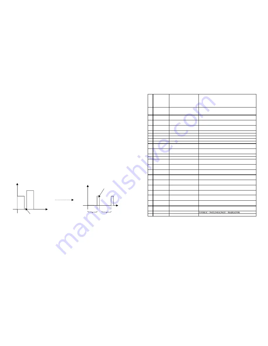
4.3.3   A/D conversion and display output circuit: The output voltage from the pin 3 of 
N419 passes through N420B where it is amplified and sent to the opposite-phase 
terminal of N420A. N420A composes a voltage comparer. We'll discuss its detailed 
working process according the voltage comparing characteristics (When the in-phase 
end's voltage is higher than that of the opposite-phase end, the output is the positive 
power. When the in-phase end's voltage is lower than that of the opposite-phase end, 
the output is the negative power.) and the figure 4.

When the opposite-phase end has a DC voltage representing 35Hz signal amplitude, 
the output of N420A is a low level close to the negative power supply. At the same time, 
+5V provides conditions for V436 to be conductive and a high level from the collector 
of V436 charges C530. The positive end's voltage of C530 (i.e. the in-phase end of 
N420A) is increasing gradually. When the voltage reach that of the opposite-phase 
end, the voltage comparer will overturn. Therefore, N420 sends out a high level close 
to the positive power supply voltage. When the comparer overturns, CPU will 
terminate the 35Hz level selection and switch to the next frequency 100Hz. During the 
switch interval, an instantaneous high level from the pin 1 of CPU makes V435 
conductive and the voltage of C530 will be released. The in-phase end of N420A will 
be charged from 0 level to 100Hz. When 100Hz charge is finished, it will switch to the 
next frequency. The process is circulated under CPU's control. The charging time from 
the 0 level to overturn represent current frequency's signal amplitude. The amplitude 
is large, time is longer; the amplitude is small, time is shorter. We can conclude from 
the above circuit working process: An analog series of DC level which has concrete 
voltage value originally becomes two mode of 0 and 1. Its time period represents the 
digital pulse of the original information. That is to say, it finishes the analog-to-digital 
conversion process. The digital pulse sent out from the output terminal of N420A 
reaches the pin 12 of CPU after opposite-phased by V437. And then CPU processes 
it and sends it to front panel display IC N901 which will make dynamic spectrum 
display on the display. As a matter of fact, every frequency is displayed sequentially. 
However, what we see on the display screen is the working process all the spectrums 
are displayed simultaneously due to every frequency display circulate very quickly. 

V


T


3

5HZ


100HZ


Switch time interval


V


T


35HZ


100HZ


Charge time

Charge time


High level 
discharge


(Figure 4)

- 20 -

127

CONNECTION
CORDS

¦ µ

0.6  SHAPED 10mm

W4,W6,W7,W9,W13,W17,W23,W25,W29,W31,W32,W35,
W40,W41,W44~W47,W54,W55,W62,W65,W80,W90,W97,
W103,W111,W112,W117,W121,W122,W133,W137,W142,
W143,W154,W163,W167,W168,W174,W177,W178,W180,
W181,W185,W186,W190,W207,W208,W209,W37

128

CONNECTION
CORDS

¦ µ

0.6  SHAPED 12.5mm

W57,W60,W67,W68,W70,W71,W77,W93,W104,
W120,W123,W124,W128,W130,W131,W144,W145,W148,
W204

129

CONNECTION
CORDS

¦ µ

0.6  SHAPED 15mm

W83,W85,W86,W107,W115,W126,W129,W146,W147,
W169~W173,W175,W176,W182,W183,W191,W201,W82

130

CONNECTION
CORDS

¦ µ

0.6  SHAPED 20mm

W33,W34,W48,W51,W114,W132,W134,W141,W166,W192,
W196,W200,W203

131 CABLE

20# 60mm BLACK WITH CHIP
SOLDER

GROUND WIRE

132 CABLE

18# 70mm BLACK

XJ1~XJ2

CABLE

22

£ £

  80mm  BLACK

XJ1~XJ2

133 FUSE TUBE

T6.3AL 250V

FL403,FL404

134 FUSE TUBE

T4AL 250V

FL405,FL401,FL402

135 FUSE HOLDER

BLX-2

FL405

136

RADIATOR
BOARD

30×16×16 AB207

SRQ401

137

LARGE
RADIATOR

267.5×91×70  AV210

CONNECTED TO THE MAIN AMPLIFICATION BOARD

138 FUSE HOLDER

0 FL401~FL404

139 SMALL CHIP

AB207

FIX TRIODE

140

ANGLE
ALUMINUM

90×23.2×30  AV210

POWER IC / LARGE RADIATOR

141

TAPPING
SCREW

BT 3×8 BLACK

2 FOR RADIATOR BOARD/MAIN AMPLIFICATION BOARD,
1 FOR N412/RADIATOR BOARD

142

TAPPING
SCREW

PB 3×12H COLOR ZINC

2 FOR SMALL CHIP/LARGE RADIATOR, 5 FOR ANGLE
ALUMINUM/LARGE RADIATOR

143

TAPPING
SCREW

PWT 3×8×8 COLOR ZINC

1 FOR MAIN AMPLIFICATION/RADIATOR, GROUNDED

144

TAPPING
SCREW

BT 3×8H COLOR ZINC

1 FOR MAIN AMPLIFICATION/RADIATOR, 3 FOR ANGLE
ALUMINUM/POWER IC

145

MACHINE
SCREW

PWM 3×16×8 COLOR ZINC

4 FOR POWER TUBE/LARGE RADIATOR

146 SCREW NUT

M3

147

SCREW
SPACER

¦ µ

3×7.2×0.5

148

SPRING
SPACER

¦ µ

3

149

INSULATION
RING

¦ µ

3×6×3

N413~N415

150 MICA SPACER

18

×

13

×

0. 1

151 MICA SPACER

22

×

19

×

0. 1

4 FOR POWER TUBE / RADIATOR

Summary of Contents for AV210

Page 1: ...ENGLISH AV210 SERVICE MANUAL ...

Page 2: ... r o c e s s i n g a n d E Q a d j u s t m e n t c ir c u it s 3 I n p u t s ig n a l s d e t e c t s e a r c h a n d f r e q u e n c y s p e c t r u m s a m p l i n g c ir c u it s 4 C o n t r o l C i r c u it 1 1 3 3 4 8 10 12 12 16 24 24 25 27 CAUTIONS There is high voltage inside this unit Make sure to pull out the plug of this unit before repairing There are many high voltage components insid...

Page 3: ...ified by N407A and N407B At the same time the pin 32 of CPU N422 sends out a high level to the electronic switch N410 s pins 9 10 and 11 SEL control signal C SR and SL signals are sent out from the N410 s pins 14 15 and 4 to IC N402 where separate volumes are adjusted SW signals D SW is sent to the IC N402 s where the volume is adjusted Therefore the 6 channel signals of 5 1 CH input are selected ...

Page 4: ...ent out from the pin 4 is added to the pin 6 of N402 where the electronic volume is adjusted The pins 10 11 SWLL are high level According to the real value table the central channel signal S C sent out from the pin 14 of N411 and the surround channel signal S S sent out from the pin 15 of N411 are added to the pins 12 2 and 5 of N410 The S S is divided into two signalssurround left and surround ri...

Page 5: ...d of N403A SEARCH is connected to the pin 28 of CPU This control signal is the search and detect signal when it is low level it enters the search mode when it is high level it stops searching Its works as follows 3 1 1 When this unit is getting started the A B control signals from the pins 38 39 in the domination of the CPU s inter program are added to the input select circuit to search circularly...

Page 6: ...d to finish the control functions RP901 finishes the master volume adjustment and RP905 finishes multi function adjustment To Encoder Master R621 680K R618 100K R619 1K R626 1K R622 1K R627 5 6K R623 10k R625 2 2K R620 10K 12V 12V R613 10K R608 10K R603 10K R598 10K R593 10K C524 223 C515 272 C518 682 C521 683 C527 154 R596 1K R597 10K R601 1K R602 10K R594 5 6K R599 5 6K R604 5 6K R609 5 6K R614 ...

Page 7: ...421 2N5401 V422 2N5401 V424 A1694 V418 2N5551 V414 2N5551 V423 C4467 V415 2N5551 V416 2N5401 R430 1K C415 10u 16V R431 47K C416 221 R432 2 7K R434 47 R433 2 7K R446 33K R437 1K C417 100U 16V R435 47 R436 620 R438 33K R439 1k R440 200 C418 33 R443 200 VD406 1N4148 V420 2N5551 V419 2N5551 R445 10 R444 10 R450 10 R449 10 R448 100 0 25W R447 100 0 25W R441 4 7K R442 2K C419 104 C413 100U 50V C412 104 ...

Page 8: ...u 16V C491 4 7u 16V C490 4 7u 16V C489 4 7u 16V C486 4 7u 16V C485 4 7u 16V C484 822 C483 153 C482 334 C487 104 TAPE R VCD L CD R VCD R CD L 5 1CH R 5 1CH L TAPE L X0 12 X1 14 X2 15 X3 11 Y0 1 Y1 5 Y2 2 Y3 4 INH 6 A 10 B 9 VEE 7 X 13 Y 3 16 8 N401 CD4052 C464 47u 16V R530 470 VD432 6 8V VD431 6 8V R529 470 C462 47u 16V 12V 12V R531 1k R532 1k REC R REC L C465 10u 16V C466 10u 16V R527 47k R528 47k...

Page 9: ...reaches the pin 12 of CPU after opposite phased by V437 And then CPU processes it and sends it to front panel display IC N901 which will make dynamic spectrum display on the display As a matter of fact every frequency is displayed sequentially However what we see on the display screen is the working process all the spectrums are displayed simultaneously due to every frequency display circulate ver...

Page 10: ...D DIP N403 N408 N420 IC 4558C DIP N403 N408 N420 105 IC L7812CV GOLD SEALED TO 220 N412 IC LM7812 GOLD SEALED TO 220 N412 106 IC CD4051 DIP N416 N419 107 IC CD4053BCN DIP N410 N411 108 IC CD4052BCN DIP N401 109 IC M62446FP SOP N402 110 IC 24C02 DIP N421 111 I C LM1875T T05B N413 N414 N415 112 SOFTWARE PROGRAM CPU CPU AV210 RU 0 N422 113 CRYSTAL OSCILLATOR 12 00MHz 49 U G601 114 RELAY JH1806 012 3H...

Page 11: ...o is e is f ilt e r e d b y t h e s h o r t c ir c u it W h e n t h e m ic r o p h o n e i s in s e r t e d t h e c o n t a c t c h ip i s c u t o f a n d t h e m ic r o p h o n e c ir c u it h a s n o r m a l o u t p u t N905 PT2399 Echo Processing Automatic Search Detect Circuit V902 AMP N404B N405B Mix with the channels L R N904B RP903 RP904 Figure 6 OK ªMUTE 18 59 PORCELAIN CAPACITOR 50V 683 1...

Page 12: ... power amplification section when the temperature rises 6 2 C SR and SL power amplification circuit These three channels employ the exclusive power amplifier IC LM1875 or TDA2030 It has five pins and is a good power amplifier IC The application circuit is very simple It has 15W power output in the rated condition The pins 5 3 are the positive negative power supplying pins and employ 2 À 2 V T h e ...

Page 13: ...8 When there is one output mid point DC voltage which is higher than 3 5V or lower than 3 5V V429 and V428 are conducted Their base voltage will decrease and V430 is conducted At last the relay switches off and the protection circuit is getting started One over voltage sampling resistor is connected to every R478 connected to L channel Above 3 5V Below 3 5V V429 conducted V428 conducted Collector ...

Page 14: ...BON FILM RESISTOR 1 6W3 3K 5 SHAPED 7 5 R948 13 CARBON FILM RESISTOR 1 6W220K 5 SHAPED 7 5 R962 14 CARBON FILM RESISTOR 1 6W30K 5 SHAPED 7 5 R936 R942 15 CARBON FILM RESISTOR 1 6W8 2K 5 SHAPED 7 5 R937 R939 R934 16 CARBON FILM RESISTOR 1 2W100 5 SHAPED 12 5 R915 CARBON FILM RESISTOR 1 6W56K 5 SHAPED 7 5 R908 17 CARBON FILM RESISTOR 1 6W47 5 SHAPED 7 5 R909 18 CARBON FILM RESISTOR 1 6W470K 5 SHAPED...

Page 15: ...5 T2 2P SHIELD WITH L NEEDLE 4 GROUND PINS XP5 59 RAFT CORDS 9P330 2 5 2 PLUG WITH L NEEDLE XP4 60 RAFT CORDS 4P60 2 5 2 PLUG 3P SHIELD WITH L NEEDLE XP6 61 INFRARED SENSOR HS0038B N902 62 SOFT SPONGE SPACER 10 10 10 DOUBLE FACED HARD N902 PCB 63 SOFT SPONGE SPACER 10 10 5 DOUBLE FACED HARD VFD901 PCB SCHEMATIC DIAGRAM OF THE FRONT CONTROL PANEL BOARD SW1 1 SW2 2 SW3 3 SW4 4 DOUT 5 DIN 6 NC 7 CLK ...

Reviews: