background image


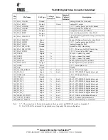
FLI2300 Digital Video Converter Data Sheet


*** Genesis Microchip Confidential *** 

PRELIMINARY INFORMATION -- SUBJECT TO CHANGE 

1 DESCRIPTION 

The FLI2300 is a highly integrated digital video 
format converter for CRT-TV applications using 
patented deinterlacing and post processing algorithms 
from Faroudja Laboratories, coupled with highly 
flexible scaling, a wide variety of aspect ratio 
conversions, and other special video enhancing 
features to produce the highest quality image. 

1.1 Inputs 


• 

Input all industry standard and non-standard 
video resolutions, including 480i (NTSC), 576i 
(PAL/SECAM), 480p, 720p, 1080i, and VGA to 
XGA 

• 

Digital input, 8-bit Y/Cr/Cb (ITU-R BT656), 8-
bit Y/Pr/Pb, 16-bit Y Cr/Cb (ITU-R BT601), 24-
bit RGB, YCrCb, YPrPb 

• 

Input pixel rate up to 75MHz maximum 

 
1.2 Outputs 

• 

Output resolutions include 480p, 576p, 720p, 
1080i, 1080p, and VGA to SXGA


• 

Interlaced or Progressive output


• 

The output can be either analog YUV/RGB 
through the integrated 10-bit Digital-To-Analog 
Converter (DAC), or digital 24-bit RGB, YCrCb, 
YPrPb (4:4:4), or digital 16/20-bit Y Cr/Cb 
(4:2:2) Output pixel rate up to 150 MHz 
maximum 

 
1.3 Formats 

• 

Input color manipulation matrix supports all 
color spaces:  RGB, YPrPb, 4:4:4 YCrCb, 4:2:2 
YCr/Cb, ITU-R BT656, ITU-R BT601 

• 

Output supports analog RGB, YPrPb, and 
YCrCb; 


• 

Output supports digital RGB, YPrPb, 4:4:4 
YCrCb and 4:2:2 YCr/Cb 

 
1.4  Frame Rate Conversion 

• 

Tearless Frame Rate Conversion 
50/60/72/75/100/120 Hz 


1.5  Front End Processing 

• 

Motion Adaptive Noise Reduction - Improves 
picture quality for off-air material. 

• 

Cross Color Suppressor (CCS) - Removes cross 
color artifacts in composite video signals due to 
poor Y/C separation in standard 2-D video 
decoders, eliminating the need for expensive 3-D 
video decoders. 

 
1.6 Deinterlacing 

• 

Per-pixel Motion Adaptive Deinterlacing 

• 

Patented FilmMode Processing - Used for proper 
de-interlacing of 3:2 and 2:2 pulldown material. 

• 

Edit Correction - Film content is continuously 
monitored for any break in sequence caused by 
“bad edits” and quickly compensates for the 
most effective reduction in artifacts. 

• 

DCDi™ by Faroudja - Video is analyzed on a 
single pixel granularity to detect presence or 
absence of angled lines and edges, which are 
then processed to produce a smooth and natural 
looking image without visible artifacts or 
“jaggies”. 

 
1.7 Scaling 

• 

High Quality Fully Programmable Two 
Dimensional Scaler 

• 

Aspect Ratio Conversion for “Anamorphic” or 
“Panoramic” (non-linear) 

• 

Display 4:3 images on 16:9 displays and vice 
versa, including Letterbox to Fullscreen, 
Pillarbox, and Subtitle Display Modes 

• 

Pixel and line dropper to generate PIP windows 

 
1.8 TrueLife™ 

Enhancer 

• 

Two dimensional, non-linear, luma and chroma 
video enhancer brings out details in the picture, 
producing a more life-like image.  

 
1.9 Memory 

• 

32-bit wide SDRAM (i.e. one 2M x 32-bit) 
controller, up to 166 MHz operation, for external 
SDRAM 

Summary of Contents for DV985S

Page 1: ...SERVICE MANUAL DV985S...

Page 2: ...VIEW AND PART LIST 4 BRACKET EXPLOSED VIEW AND PART LIST 6 ELECTRICAL CONFIRMATION 8 VI DEO OUTPUT LUMINANCE SIGNAL CONFIRMATION 8 VI DEO OUTPUT CHROMINANCE SIGNAL CONFIRMATION 9 MPEG BOARD CHECK WAV...

Page 3: ...removing an electrical assembly equipped with ES devices place the assembly on a conductive surface such as alminum foil to prevent electrostatic charge buildup or exposure of the assembly 3 Use only...

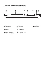
Page 4: ...Front Panel Illustration POWER switch Disc tray STOP button IR SENSOR Display window OPEN CLOSE button 6 5 4 2 3 7 2 7 6 PLAY PAUSE button 3 4 5...

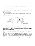
Page 5: ...installation the both ends of the laser diode are short circuited After replacing the parts with new ones remove the short circuit according to the correct procedure See this Technical Guide 2 Do not...

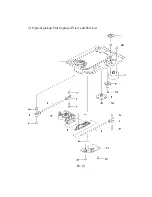
Page 6: ...5 1 Optical pickup Unit Explosed View and Part List Pic 1...

Page 7: ...MIDDLE A 1 7 1EA2511A29400 GEAR MIDDLE B 1 8 1EA2744A03000 SHAFT SLIDE 1 9 1EA2744A03100 SHAFT SLIDE SUB 1 10 1EA2812A15300 SPRING COMP TYOUSEI 3 11 1EA2812A15400 SPRING COMP RACK 1 21 1EA0B10B20100 A...

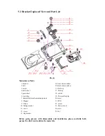
Page 8: ...t wheel 17 Pick up 5 gearwheel 18 switch 6 iron chip 19 Five pin flat plug 7 Immobility mechanism equipment 20 screw 8 Magnet 21 PCB 9 Platen 22 motor 10 Bridge bracket 23 Motor wheel 11 screw 24 scre...

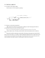
Page 9: ...h a soldering iron after a circuit is connected Keep the power source of the pick up protected from internal and external sources of electrical noise Refrain from operation and storage in atmospheres...

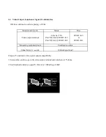
Page 10: ...onnect the oscilloscope to the video output terminal and terminate at 75 ohms 2 Confirm that luminance signal Y S level is 1000mVp p 30mV Measurement point Video output terminal Color bar 75 PLAY Titl...

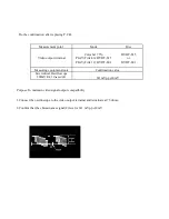
Page 11: ...tput terminal and terminate at 75 ohme 2 Confirm that the chrominance signal C level is 621 mVp p 30mV Measurement point Video output terminal Color bar 75 PLAY Title 46 DVDT S15 PLAY Title 12 DVDT S0...

Page 12: ......

Page 13: ...and 4 2 2 YCr Cb 1 4 Frame Rate Conversion Tearless Frame Rate Conversion 50 60 72 75 100 120 Hz 1 5 Front End Processing Motion Adaptive Noise Reduction Improves picture quality for off air material...

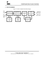
Page 14: ...ut Processor with Auto Sync and auto Adjust Noise Reducer Deinterlacer Frame Rate Converter and SDRAM interface Port 2 8 bit 656 Input Port 1 8 16 24 bit RGB YCrCb Input Clock Generation PLLs 2Mx32 SD...

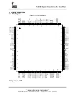
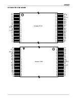
Page 15: ...ATA 30 SDRAM DATA 29 SDRAM DATA 28 SDRAM DATA 26 SDRAM DATA 27 SDRAM DATA 25 SDRAM DATA 24 SDRAM DATA 23 SDRAM DATA 21 SDRAM DATA 22 VDDcore4 VSScore VSS VDD5 TEST IN SDRAM ADDR 10 SDRAM ADDR 5 SDRAM...

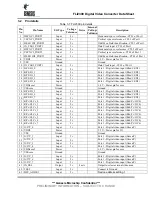
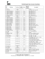
Page 16: ...18 B Cb D1_5 Input 5v Port 1 Digital video input Blue Cb D1 19 B Cb D1_6 Input 5v Port 1 Digital video input Blue Cb D1 20 B Cb D1_7 Input 5v Port 1 Digital video input Blue Cb D1 21 R Cr Cb Cr_0 Inpu...

Page 17: ...r pin for IO 63 VSS Ground Ground 64 SDRAM DATA 12 Tristate I O 5v 4 mA PD SDRAM data bus 65 SDRAM DATA 13 Tristate I O 5v 4 mA PD SDRAM data bus 66 SDRAM DATA 14 Tristate I O 5v 4 mA PD SDRAM data bu...

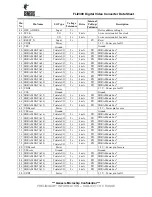
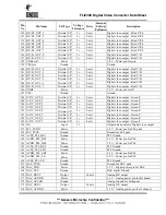
Page 18: ...BA1 Tristate O P 5v 8 mA SDRAM bank select 1 108 SDRAM BA0 Tristate O P 5v 8 mA SDRAM bank select 0 109 SDRAM CSN Tristate O P 5v 4 mA SDRAM CS 110 SDRAM DQM Tristate O P 5v 8 mA SDRAM DQM 111 SDRAM...

Page 19: ...DD8 Power 3 3 V Power pin for IO 147 VSS Ground Ground 148 G Y Y_OUT_0 Tristate O P 5v 8 mA Digital video output Green Y 149 G Y Y_OUT_1 Tristate O P 5v 8 mA Digital video output Green Y 150 G Y Y_OUT...

Page 20: ...Test pin connect to ground 191 XTAL IN Input External parallel crystal oscillator 192 XTAL OUT Output External parallel crystal oscillator 193 VDD9 Power 3 3 V Power pin for IO 194 VSS Ground Ground 1...

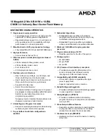
Page 21: ...r Sectors can be locked in system or via programming equipment Temporary Sector Unprotect feature allows code changes in previously locked sectors Unlock Bypass Program Command Reduces overall program...

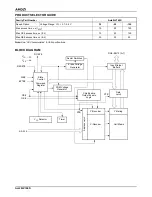
Page 22: ...ss time ns tACC 70 90 120 Max CE access time ns tCE 70 90 120 Max OE access time ns tOE 30 35 50 Input Output Buffers X Decoder Y Decoder Chip Enable Output Enable Logic Erase Voltage Generator PGM Vo...

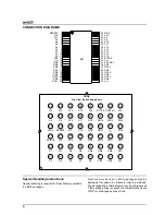
Page 23: ...12 DQ4 VCC DQ11 DQ3 DQ10 48 33 47 46 45 44 43 42 41 40 39 38 37 36 35 34 25 32 31 30 29 28 27 26 A1 A15 A18 A14 A13 A12 A11 A10 A9 A8 A19 NC WE RESET NC NC RY BY A17 A7 A6 A5 A4 A3 A2 1 16 2 3 4 5 6 7...

Page 24: ...22 RESET A18 A17 A7 A6 A5 A4 A3 A2 A1 A0 CE VSS OE DQ0 DQ8 DQ1 DQ9 DQ2 DQ10 DQ3 DQ11 44 43 42 41 40 39 38 37 36 35 34 33 32 31 30 29 28 27 26 25 24 23 WE A19 A8 A9 A10 A11 A12 A13 A14 A15 A16 BYTE VSS...

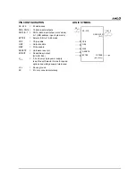
Page 25: ...16 bit mode CE Chip enable OE Output enable WE Write enable RESET Hardware reset pin RY BY Ready Busy output N A SO 044 VCC 3 0 volt only single power supply see Product Selector Guide for speed opti...

Page 26: ...f consecutive read or write cycles initiated by a single control command Burst length of 1 2 4 8 or Full page and the burst count sequence sequential or interleave A burst of read or write cycles in p...

Page 27: ...ite Enable RAS CAS and WE define the operation Refer function truth table for details LDQM UDQM Data Input Output Mask Controls output buffers in read mode and masks input data in write mode DQ0 DQ15...

Page 28: ...olumn Pre Decoders Column Add Counter Row active Column Active Burst Counter Data Out Control CAS Latency Internal Row counter DQ0 DQ1 DQ14 DQ15 refresh Self refresh logic timer Pipe Line Control I O...

Page 29: ...e 12 bit or 24 bit mode 1 pixel clock inputs Flexible Input Clocking Single clock single edge 24 bit Single clock dual edge 12 24 bit Dual clock single edge 12 bit I 2 C Slave Programming Interface up...

Page 30: ...g one or two clocks with one or two edges per clock An attached monitor may be sensed using the HTPLG pin or internally with Receiver Sense This detected state may be output onto the MSEN pin The devi...

Page 31: ...24 bit input bus widths DSEL selects between single edge and dual edge modes for the input clocks EDGE selects between rising and falling edge on the input clocks CLK and CLK provide the one or two cl...

Page 32: ...er applied 0 25 70 C JA Thermal Resistance Junction to Ambient 1 64 C W Note 1 Airflow at 0m s Digital I O Specifications Under normal operating conditions unless otherwise specified Symbol Parameter...

Page 33: ...510 510 550 590 mV VDOH Differential High level Output AVCC V Voltage 1 IDOS Differential Output Short Circuit Current 1 VOUT 0 V 5 A IPD Power down Current 2 0 2 1 0 mA ICCT Transmitter Supply Curre...

Page 34: ...HSYNC Setup Time to IDCK falling rising edge 1 Default De skew Setting Dual Edge DSEL 1 BSEL 0 0 6 ns THID Data DE VSYNC HSYNC Hold Time from IDCK falling rising edge 1 Default De skew Setting Dual E...

Page 35: ...Data Sheet Input Timing Diagrams TCIH TCIL TCIP 2 0 V 0 8 V 0 8 V 2 0 V 2 0 V Figure 3 Clock Cycle High Low Times Figure 4 Low Swing Differential Times ISEL RST VCC TRESET Figure 5 ISEL RST Minimum T...

Page 36: ...TL 3 1 Delay Time from DE DE TLDE THDE 0 8 V 2 0 V 0 8 V 2 0 V Figure 8 DE High and Low Times Figure 9 I 2 C Data Valid Delay driving Read Cycle data D 23 0 DE HSYNC VSYNC IDCK TSIDF THIDF TSIDR THIDR...

Page 37: ...n 12 bit mode when dual edge clocking is turned off DSEL LOW It is used to provide the ODD latching edges for dual clock single edge If BSEL HIGH or DSEL HIGH this pin is unused and should be tied to...

Page 38: ...then this pin selects whether single clock dual edge is used Dual Edge clock select When HIGH IDCK latches input data on both falling and rising clock edges When LOW IDCK IDCK latches input data on on...

Page 39: ...C mode Differential Signal Data Pins Pin Name Pin Type Description TX0 TX0 TX1 TX1 TX2 TX2 25 24 28 27 31 30 Analog Analog Analog Analog Analog Analog TMDS Low Voltage Differential Signal input data...

Page 40: ...en and read from are listed as R W while registers that can be read only are listed with RO 3 Actual jitter tolerance may be higher depending on the frequency of the jitter 4 Contents of this register...

Page 41: ...t data is dual edge latched HEN RW Horizontal Sync Enable 0 HSYNC input is transmitted as fixed LOW 1 HSYNC input is transmitted as is VEN RW Vertical Sync Enable 0 VSYNC input is transmitted as fixed...

Page 42: ...racteristics of PLL filter in the VDJK register 100 Recommended value SCNT RW SYNC Continuous 1 To enable recommended setting 0 To disable DK 3 1 RW De skewing Setting Increment 260psec 000 1 step min...

Page 43: ...grates the MediaTek 2nd generation front end analog RF amplifier and the Servo MPEG AV decoder The progressive scan of the MT1389 utilized a proprietary advanced motion adaptive de interlace algorithm...

Page 44: ...output or digital output Embedded Micro controller Built in 8032 micro controller Built in internal 373 and 8 bit programmable lower address port 1024 bytes on chip RAM Up to 4M bytes FLASH programmin...

Page 45: ...e echo Microphone tone control Vocal mute vocal assistant Key shift up to 8 keys Chorus Flanger Harmony Reverb Channel equalizer 3D surround processing include virtual surround and speaker separation...

Page 46: ...G12 SEG11 SEG10 SEG9 SEG8 SEG7 SEG6 SEG5 SEG4 SEG3 SEG2 SEG1 R416 10K VCC C406 101 R417 10K VCC TC402 100uF 16V TC401 100uF 16V R418 10R F1 1 F1 2 P16 4 P13 7 P14 6 P15 5 P12 8 P11 9 P10 10 P9 11 P8 1...

Page 47: ......

Page 48: ...ER105 TC513 100uF 16V D503 1N4007 D502 1N4007 D504 1N4007 D501 1N4007 C508 104 9V ZD502 9 1V 1W 2 3 4 6 7 10 11 9 12 13 14 15 16 TR501 EI128 8 2 TC515 470uF 25V D513 HER105 C516 101 R512 22K R514 10K...

Page 49: ......

Page 50: ...V985S 7969 32 DDB Drawn By SW GND K901 6x6x1 FL FL 21V GND 9V 9V GND 5V STB CPU 3 3V AGND 2 3 4 1 5 6 8 9 10 7 11 12 13 XS901 OK DET FL FL 21V GND CPU 3 3V 5V SW GND PLED1 STB PLED OLED PLED OLED 2 3...

Page 51: ......

Page 52: ...10V AGND PDAT0 V703 8050 R711 1K R712 2 2K A 10V PDAT2 C716 104 AGND VCC AGND R707 A 10V AGND AGND VCC PDAT0 10V VGND VGND Pr L709 FBSMT L708 FBSMT L707 FBSMT Y1 Pb VGND GREEN BLUE RED B G R 1 2 3 4 5...

Page 53: ......

Page 54: ...125 VSScore 124 VDDcore6 1 8 123 CTLOUT4 122 CTLOUT3 121 CTLOUT2 120 CTLOUT1 119 CTLOUT0 118 TEST OUT1 117 TEST OUT0 116 TEST3 115 SDRAM CLKIN 114 VSSio6 113 VDD6 3 3 112 SDRAM CLKOUT 111 SDRAM DQM 1...

Page 55: ......

Page 56: ...core6 1 8 123 CTLOUT4 122 CTLOUT3 121 CTLOUT2 120 CTLOUT1 119 CTLOUT0 118 TEST OUT1 117 TEST OUT0 116 TEST3 115 SDRAM CLKIN 114 VSSio6 113 VDD6 3 3 112 SDRAM CLKOUT 111 SDRAM DQM 110 SDRAM CSN 109 SDR...

Page 57: ...3 4 1 XS201 XS04 2 3 4 1 XS203 XS04 C240 104 C242 104 C230 104 C236 104 C232 104 C238 104 TC219 100uF 16V C234 104 C228 104 3 3V TC217 47uF 16V C224 104 C225 104 C226 104 C222 104 C223 104 C221 104 D...

Page 58: ...O V1P4 V1P4 ADIN L202 FB 89V33 PWR A16 A15 A14 A13 A12 A11 A10 A9 A20 PCE A1 PRD AD0 AD1 AD2 AD3 AD4 AD5 AD6 A21 AD7 A17 A0 V18 VSCK VSDA VSTB SCL SDA RXD TXD URST IR DQM0 DQS0 DQ7 DQ6 DQ5 DQ4 DQ3 DQ2...

Page 59: ...1 5 6 8 9 10 7 11 12 13 XS203 XS13 L224 FB L225 1K MUTEA ASTB MUTE_DAC AGND VGND LFE Cc SR SL Rt Lt VIDEO_COMP VIDEO_U VIDEO_V VIDEO_C VIDEO_Y VCC IEC958 2 3 4 1 5 6 8 9 10 7 11 12 14 15 16 13 17 18...

Page 60: ...2SC1815 YS C2138 104 C2139 104 C2140 104 9V AGND C2141 104 C2142 104 C2143 104 9V AGND SDATA2 SDATA1 SDATA0 SLRCK SACLK SBCLK SCL SDA RESET LL RS RR LS LFE C R2132 20K C2116 102 OKA AGND R2156 20K R2...

Page 61: ......
Page 62: ...7 C509 C511 C513 C514 19 PORCELAIN CAPACITOR 1000V 103 80 20 7 5mm 1 C502 20 TERYLENE CAPACITOR 100V 102 5 3 5mm 1 C506 21 PORCELAIN CAPACITOR 50V 104 20 5mm 7 C508 C510 C517 C515 C518 C51 9 C520 22 P...

Page 63: ...D HEAT RADIATION BOARD 58 TAPPING SCREW BT 3 8 BLACK 2 U504 U505 FOR HEAR RADIATION 59 FUSE T1 6AL 250V 1 F501 60 FUSE HOLDER BLX 2 1 FOR F501 61 POWER GROUND PIECE AB903 1 G503 62 IC LM7805 SEALEDTO...

Page 64: ...30 SOFTWARE PROGRAM EPROM ROM969S 0A 53S 1 3 OUTPUT BOARD MATERIAL SPECIFICATIONS PART NUMBER QUANTITY LOCATION 1 SMD RESISTOR 1 16W 100 5 1 R702 2 CARBON FILM RESISTOR 1 4W68 5 1 R703 3 SMD RESISTOR...

Page 65: ...ARD MATERIAL SPECIFICATIONS PART NUMBER QUANTITY LOCATION 1 SMD RESISTOR 1 16W 0 5 15 R206 R209 R226 R240 R242 R249 R 251 R253 R255 R259 R264 R265 R26 6 2 SMD RESISTOR 1 16W 33 5 5 R222 R223 R224 R225...

Page 66: ...H REFLECTIVE NEDDLE 1 XS901 3 LIGHT TOUCH RESTORE SWITCH HERIZONTAL 6 6 1 1 4 PCB 9971 0 1 5 DECODE BOARD MATERIAL SPECIFICATIONS PART NUMBER QUANTITY LOCATION 1 SMD RESISTOR 1 16W 0 5 0603 34 C2119 C...

Page 67: ...8 TC309 TC247 TC248 TC239 TC249 30 SMD CAPACITOR 50V 20P 5 NPO 0603 1 C222 31 SMD CAPACITOR 50V 27P 5 NPO 0603 2 C275 C276 32 SMD CAPACITOR 50V 47P 5 NPO 0603 17 C262 C265 C266 C289 C290 C29 2 C293 C2...

Page 68: ...06 V309 54 SMD TRIODE 9014C 1 V310 55 TRIODE 9015C 1 Q204 56 TRIODE C1815Y 1 Q212 57 SMD TRIODE C1815 6 Q205 Q210 58 TRIODE 2SA1015 3 Q211 Q218 Q219 59 SMD TRIODE 3904 1 V305 60 SMD TRIODE 3906 6 Q220...

Reviews: