SiI
164
PanelLink
PanelLink
PanelLink
PanelLink
Transmitter September 2002
Data Sheet
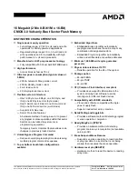
General Description
The
SiI
164 transmitter uses PanelLink
®
Digital
technology to support displays ranging from VGA to
UXGA resolutions (25 - 165Mpps) in a single link
interface.
The
SiI
164 transmitter has a highly flexible interface
with either a 12-bit mode (½ pixel per clock edge) or
24-bit mode 1 pixel per clock edge input for true color
(16.7 million) support. In 24-bit mode, the
SiI
164
supports single or dual edge clocking. In 12-bit mode,
the SiI164 supports dual edge single clocking or
single edge dual clocking. The
SiI
164 can be
programmed though an I
2
C interface. In addition the
SiI
164 also supports Receiver and Hot Plug
Detection.
PanelLink Digital technology simplifies PC design by
resolving many of the system level issues associated
with high-speed mixed signal design, providing the
system designer with a digital interface solution that is
quicker to market and lower in cost.
Features
•
Scaleable Bandwidth: 25 - 165MHz Flexible
•
Graphics Controller Interface: 12-bit or 24-bit
mode 1 pixel/clock inputs
•
Flexible Input Clocking: Single clock single
edge (24-bit), Single clock dual edge (12-/24-
bit), Dual clock single edge (12-bit)
•
I
2
C Slave Programming Interface up to 100kHz
•
Low Voltage Interface: 3.3V with option for 1.0
to 3.0V Low Voltage Signal Mode
•
Monitor Detection supported through hot plug
and receiver detection
•
De-skewing Option varies input clock to input
data timing
•
Low Power: 3.3V operation (120mA max.) and
Power Down mode (1mA max.)
•
Cable Distance Support: over 5m with twisted
pair and fiber-optics ready
•
Compliant with DVI 1.0 (DVI is backwards
compliant with VESA
®
P&D
TM
and DFP)
•
Standard and Pb-free packages (see pg 29)
SiI
164
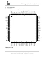
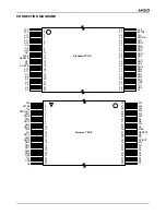
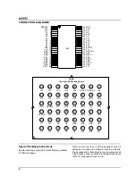
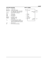
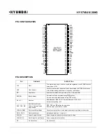
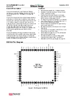
Pin Diagram
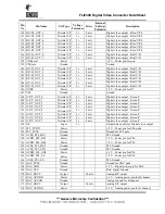
VCC
DE
VREF
HSYNC
VSYNC
CTL3/A3/DK3
CTL2/A2/DK2
CTL1/A1/DK1
EDGE/HTPLG
PD#
MSEN
VCC
ISEL/RST#
DSEL/SDA
BSEL/SCL
GND
PGND
PVCC1
EXT_SWING
AGND
TXC-
TXC+
AVCC
TX0-
TX0+
AGND
TX1-
TX1+
AVCC
TX2-
TX2+
VCC
RESERVED
DKEN
D23
D22
D21
D20
D19
D18
D17
D16
D15
D14
D13
D12
GND
PVCC2
D11
D10
D9
D8
D7
D6
IDCK-
IDCK+
D5
D4
D3
D2
D1
D0
GND
1
2
3
4
5
6
7
8
9
10
11
12
13
14
15
16
17
18
19
20
21
22
23
24
25
26
27
28
29
30
31
32
33
34
35
36
37
38
39
40
41
42
43
44
45
46
47
48
49
50
51
52
53
54
55
56
57
58
59
60
61
62
63
64
SiI
164
64-Pin TQFP
(Top View)
AGND
Figure 1. Pin Diagram for
SiI
164
Summary of Contents for DV985S
Page 1: ...SERVICE MANUAL DV985S...
Page 6: ...5 1 Optical pickup Unit Explosed View and Part List Pic 1...
Page 12: ......
Page 47: ......
Page 49: ......
Page 51: ......
Page 53: ......
Page 55: ......
Page 61: ......

