SiI
164
PanelLink
Transmitter
Data Sheet
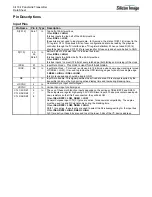
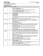
Pin Descriptions (cont’d)
Configuration Pins
Pin Name Pin # Type Description
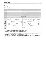
MSEN 11
Out
Monitor Sense. This pin is an open collector output. The behavior of this output depends on
whether I
2
C interface active:
I
2
C bus inactive (ISEL/RST# = LOW)
HIGH level indicates a powered on receiver is detected at the differential outputs.
A LOW level indicates a powered on receiver is not detected.
I
2
C bus is enabled (ISEL/RST# = HIGH)
The output is programmable through the I
2
C interface (see I
2
C Register Definitions).
An external 5K pull-up resistor to VDDQ is required on this pin.
ISEL/RST# 13 In I
2
C Interface Select.
ISEL/RST#=HIGH
,
I
2
C interface is active.
ISEL/RST#=LOW
,
I
2
C is inactive and the chip configuration is read from the configuration strapping pins. This pin
also acts as an asynchronous reset to the I
2
C interface controller. The reset is active when this
input is held LOW.
Note
: When the I
2
C interface is active, DKEN must be set HIGH.
BSEL/SCL 15 In Input bus select / I
2
C clock. This pin is an open collector input. If I
2
C bus is enabled
(ISEL/RST# = HIGH), then this pin is the I
2
C clock input. If the I
2
C is disabled (ISEL/RST# =
LOW), then this pin selects the input bus width.
Input Bus Select:
HIGH selects 24-bit input mode
LOW selects 12-bit input mode
DSEL/SDA 14 In/Out
Dual edge clock select / I
2
C Data. This pin is an open collector input/output. If I
2
C bus is
enabled (ISEL/RST# = HIGH), then this pin is the I
2
C data line. If the I
2
C bus is disabled
(ISEL/RST# = LOW), then this pin selects whether single clock dual edge is used.
Dual Edge clock select:
When HIGH, IDCK+ latches input data on both falling and rising clock edges.
When LOW, IDCK+/IDCK- latches input data on only falling or rising clock edges.
In 24-/12-bit mode:
If HIGH (dual edge), IDCK+ is used to latch data on both falling and rising edges.
If LOW (single edge), IDCK+ latches 1
st
half data and IDCK- latches 2
nd
half data.
EDGE/
HTPLG
9 In
Edge select / Hot Plug input. If the I
2
C bus is enabled (ISEL/RST# = HIGH), then this pin is
used to monitor the “Hot Plug” detect signal (Please refer to the DVI
TM
or VESA
®
P&D
TM
and
DFP standards). This Input is ONLY 3.3V tolerant and has no internal de-bouncer circuit.
If I
2
C bus is disabled (ISEL/RST# = LOW), then this pin selects the clock edge that will latch
the data. How the EDGE setting works depends on whether dual or single edge latching is
selected:
Dual Edge Mode (DSEL = HIGH)
EDGE = LOW, the primary edge (first latch edge after DE is asserted) is the falling edge.
EDGE = HIGH, the primary edge (first latch edge after DE is asserted) is the rising edge.
Note:
In 24-bit Single Clock Dual Edge mode, EDGE is ignored.
Single Edge Mode (DSEL = LOW)
EDGE = LOW, the falling edge of the clock is used to latch data.
EDGE = HIGH, the rising edge of the clock is used to latch data.
DKEN 35 In
De-skewing enable.
I
2
C mode (ISEL/RST# = HIGH)
DKEN pin must be set to HIGH. DK[3:1] pins are ignored and the De-skewing increments are
selected through the I
2
C interface (see the I
2
C register definitions).
Non I
2
C mode (ISEL/RST# = LOW)
DKEN = LOW, then default De-skewing setting is used.
DKEN = HIGH, then DK[3:1] is used as the De-skewing setting. The De-skewing increments
are T
STEP
. Please see Data De-skew Feature for an illustration.
Summary of Contents for DV985S
Page 1: ...SERVICE MANUAL DV985S...
Page 6: ...5 1 Optical pickup Unit Explosed View and Part List Pic 1...
Page 12: ......
Page 47: ......
Page 49: ......
Page 51: ......
Page 53: ......
Page 55: ......
Page 61: ......

