SiI
164
PanelLink
Transmitter
Data Sheet
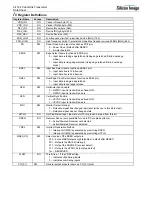
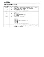
Pin Descriptions (cont’d)
Input Voltage Reference Pin
Pin Name Pin # Type
Description
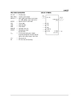
VREF
3
Analog In Input Reference Voltage. Selects the Swing range of the digital inputs, which include only
D[23:0], IDCK+, IDCK-, DE, VSYNC, and HSYNC. Input pins SCL and SDA, RST, BSEL,
DSEL, EDGE and PD# require 3.3V high swing signals and are not changed by the VREF
input.
To set the digital inputs to 3.3V High Voltage Swing, VREF must be set to 3.3V.
To set the digital inputs to Low Voltage Swing, VREF must be set to ½ of VDDQ where
VDDQ is swing level of input signal. Thus for DVO mode(1.5V Low Voltage Swing) VREF
should be set to 0.75V and BSEL=LOW.
Power Management Pins
Pin Name Pin #
Type
Description
PD# 10 In Power Down (
active
LOW
). A
HIGH
level indicates normal operation. A
LOW
level
indicates Power Down mode. In Power Down mode the Analog core is disabled and Output
buffers/pins are tri-stated however the Input buffer/pins and I
2
C Block for read and write are
active. PD# pin is disabled during I
2
C mode. PD# should be tied low during I
2
C mode.
Differential Signal Data Pins
Pin Name
Pin #
Type
Description
TX0+
TX0-
TX1+
TX1-
TX2+
TX2-
25
24
28
27
31
30
Analog
Analog
Analog
Analog
Analog
Analog
TMDS Low Voltage Differential Signal input data pairs.
These pins are tri-stated when PD# is pulled low.
TXC+
TXC-
22
21
Analog
Analog
TMDS Low Voltage Differential Signal input clock pair.
These pins are tri-stated when PD# is pulled low.
EXT_SWING
19
Analog Voltage Swing Adjust. A resistor should tie this pin to AVCC. This resistor sets the
amplitude of the voltage swing. A smaller resistor value sets a larger voltage swing and
vice versa. For remote display applications a 510
Ω
resistor is recommended. While for
notebook computers 680
Ω
is recommended to ensure voltage swing is not overdriven
over a short cable distance.
Reserved Pins
Pin Name
Pin # Type Description
RESERVED 34 In Must be tied
LOW
for normal operation.
Power and Ground Pins
Pin Name
Pin #
Type
Description
VCC
1,12,33
Power
Digital VCC, must be set to 3.3V nominal.
GND 16,48,64 Ground
Digital
GND.
AVCC
23,29
Power
Analog VCC, must be set to 3.3V nominal.
AGND 20,26,32 Ground
Analog
GND.
PVCC1
18
Power
Primary PLL Analog VCC, must be set to 3.3V nominal.
PVCC2
49
Power
Filter PLL Analog VCC, must be set to 3.3V nominal.
PGND
17
Ground
PLL Analog GND.
Summary of Contents for DV985S
Page 1: ...SERVICE MANUAL DV985S...
Page 6: ...5 1 Optical pickup Unit Explosed View and Part List Pic 1...
Page 12: ......
Page 47: ......
Page 49: ......
Page 51: ......
Page 53: ......
Page 55: ......
Page 61: ......

