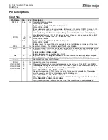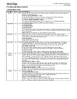
SiI
164
PanelLink
Transmitter
Data Sheet
I
2
C Registers
I
2
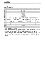
C Register Mapping
Addr.
Bit 7
Bit 6
Bit 5
Bit 4
Bit 3
Bit 2
Bit 1
Bit 0
0x00
VND_IDL (RO)
0x01
VND_IDH (RO)
0x02
DEV_IDL (RO)
0x03
DEV_IDH (RO)
0x04
DEV_REV (RO)
0x05
RSVD[7:0]
0x06
FRQ_LOW (RO)
0x07
FRQ_HIGH (RO)
0x08
RSVD[1:0] VEN
(R/W)
HEN
(R/W)
DSEL (RW) BSEL (RW) EDGE (RW)
PD (RW)
0x09
VLOW (RO)
MSEL[2:0] (RW)
TSEL (RW) RSEN (RO)
HTPLG
(RO)
MDI (RW)
0x0A
DK[3:1] (RW)
DKEN (RW)
CTL[3:1] (RW)
RSVD
0x0B
CFG[7:0]
4
(RO)
0x0C
7
SCNT
(RW)
RSVD
PLLF[3:1]
(RW)
PFEN
(RW)
0x0D
RSVD[3:0]
RSVD[3:0]
0x0E
RSVD[7:0]
0x0F
RSVD[7:0]
Notes
1. All values are Bit 7(MSB) and Bit 0(LSB).
2. Registers that can be written and read from are listed as (R/W) while registers that can be read only are listed with (RO).
3. Actual jitter tolerance may be higher depending on the frequency of the jitter.
4. Contents of this register are dependent on the status of pins D[23:16].
5. After the RESET signal is deasserted in I
2
C mode, only PD and MSEL have a default value or can retain their
programmed value set before the reset. All other registers do not have a default value or retain their value after a reset.
As such all required registers other than PD and MSEL must reinitialized in I
2
C mode after being powered up or reset.
6. Registers listed as RSVD are reserved and for Silicon Image, Inc use only.
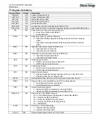
7. 0x0C is also called the
VDJK
Register. Default setting for the VDJK register 0x0C is 89h, which is optimum for most
applications.
Summary of Contents for DV985S
Page 1: ...SERVICE MANUAL DV985S...
Page 6: ...5 1 Optical pickup Unit Explosed View and Part List Pic 1...
Page 12: ......
Page 47: ......
Page 49: ......
Page 51: ......
Page 53: ......
Page 55: ......
Page 61: ......

