SiI
164
PanelLink
Transmitter
Data Sheet
I
2
C Register Definitions
Register Name
Access
Description
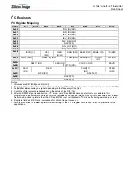
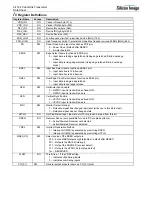
VND_IDL
RO
Vendor ID Low byte (01h)
VND_IDH
RO
Vendor ID High byte (00h)
DEV_IDL
RO
Device ID Low byte (06h)
DEV_IDH
RO
Device ID High byte (00h)
DEV_REV
RO
Device Revision (00h)
FRQ_LOW
RO
Low frequency limit at 1-pixel/clock mode (MHz) (19h)
FRQ_HIGH
RO
High frequency limit at 1-pixel/clock mode Max frequency minus 65MHz (MHz) (64h)
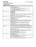
PD
RW
Power Down mode (same function as PD# pin)
0 – Power Down (Default after RESET)
1 – Normal operation
EDGE
RW
Edge Select (same function as EDGE pin)
0 – Input data is falling edge latched (falling edge latched first in dual edge
mode)
1 – Input data is rising edge latched (rising edge latched first in dual edge
mode)
BSEL
RW
Input Bus Select (same function as BSEL pin)
0 – Input data bus is 12-bits wide
1 – Input data bus is 24-bits wide
DSEL
RW
Dual Edge Clock Select (same function as DSEL pin)
0 – Input data is single edge latched
1 – Input data is dual edge latched
HEN
RW
Horizontal Sync Enable:
0 – HSYNC input is transmitted as fixed LOW
1 – HSYNC input is transmitted as is
VEN
RW
Vertical Sync Enable:
0 – VSYNC input is transmitted as fixed LOW
1 – VSYNC input is transmitted as is
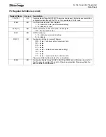
MDI
RW
Monitor Detect Interrupt
0 – Detection signal has changed logic level (write one to this bit to clear)
1 – Detection signal has not changed state
HTPLG
RO
Hot Plug Detect input, the state of HTPLG pin can be read from this bit
RSEN
RO
Receiver Sense (only available for use in DC coupled systems)
0 – Active/Powered Receiver not detected
1 – Active/Powered Receiver detected
TSEL
RW
Interrupt Generation Method
0 – Interrupt bit (MDI) is generated by monitoring RSEN
1 – Interrupt bit (MDI) is generated by monitoring HTPLG
MSEL[2:0]
RW
Select source of the MSEN output pin
000 – Force MSEN outputs high (disabled – default after RESET)
001 – Outputs the MDI bit (interrupt)
010 – Output the RSEN bit (receiver detect)
011 – Outputs the HTPLG bit (hot plug detect)
1xx – RESERVED
VLOW
RO
This bit is a 1 if the VREF setting
1 – Indicates High Swing inputs
0 – Indicates Low Swing inputs
CTL[3:1]
RW
General purpose inputs (same as CTL[3:1] pins)
Summary of Contents for DV985S
Page 1: ...SERVICE MANUAL DV985S...
Page 6: ...5 1 Optical pickup Unit Explosed View and Part List Pic 1...
Page 12: ......
Page 47: ......
Page 49: ......
Page 51: ......
Page 53: ......
Page 55: ......
Page 61: ......

