SLUS530D − SEPTEMBER 2002 − REVISED SEPTEMBER 2003
www.ti.com
11
FUNCTIONAL DESCRIPTION
TEMPERATURE QUALIFICATION
NOTE:The temperature qualifications apply only to versions with temperature sense input (TS) pin option (bq24010 and
bq24014).
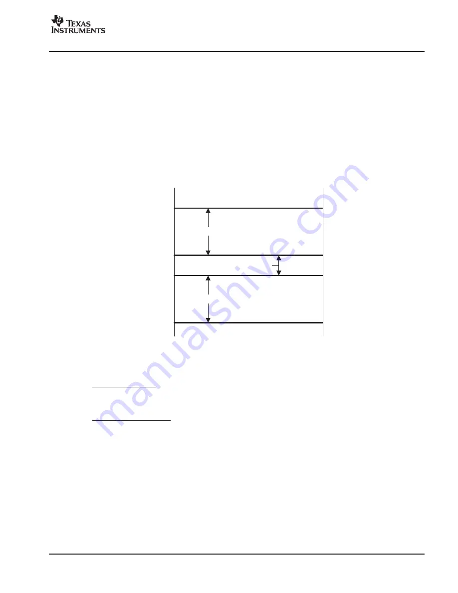
Versions of the bqTINY with the TS pin option, continuously monitor battery temperature by measuring the voltage between
the TS and VSS pins. A negative temperature coefficient thermistor (NTC) and an external voltage divider typically
develops this voltage (see Figure 3). The bqTINY compare this voltage against the internal V
(TS1)
and V
(TS2)
thresholds
to determine if charging is allowed (see Figure 6). The temperature sensing circuit is immune to any fluctuation in V
CC
since
both the external voltage divider and the internal thresholds are ratiometric to V
CC
.
Once a temperature outside the V
(TS1)
and V
(TS2)
thresholds is detected the bqTINY immediately suspend the charge. The
bqTINY suspends charge by turning off the powerFET and holding the timer value (i.e. timers are NOT reset). Charge is
resumed when the temperature returns to the normal range.
Charge Suspend
Normal Temperature Range
Charge Suspend
V(TS2)
V(TS1)
VSS
VCC
Figure 6. TS Pin Thresholds
The resistor values of R
T1
and R
T2
are calculated by equations (1) and (2) (for NTC Thermistors )
R
T1
+
ǒ
5
R
TH
R
TC
Ǔ
ǒ
3
ǒ
R
TC
*
R
TH
Ǔ
Ǔ
R
T2
+
ǒ
5
R
TH
R
TC
Ǔ
ǒ
2
R
TC
Ǔ
*
ǒ
7
R
TH
Ǔ
Where R
TC
is the cold temperature resistance and R
TH
is the hot temperature resistance of thermistor, as specified
by the thermistor manufacturer.
R
T1
or R
T2
can be omitted If only one temperature (hot or cold) setting is required. Applying a constant voltage
between the V
TS1
and V
TS2
thresholds to pin TS disables the temperature-sensing feature.
(1)
(2)
Summary of Contents for PV420S
Page 1: ...SERVICE MANUAL PV420S WWW BBK RU ...
Page 72: ... 69 CXD3068Q Block Diagram ...
Page 73: ... 70 CXD3068Q Pin Configuration ...
Page 122: ... 119 CXD3068Q Timing Chart 1 3 ...
Page 123: ... 120 CXD3068Q Timing Chart 1 4 ...
Page 124: ... 121 CXD3068Q Timing Chart 1 5 ...
Page 129: ... 126 CXD3068Q Timing Chart 2 1 ...
Page 130: ... 127 CXD3068Q Block Diagram 2 2 ...
Page 131: ... 128 CXD3068Q Timing Chart 2 3 ...
Page 134: ... 131 CXD3068Q Timing Chart 2 6 ...
Page 138: ... 135 CXD3068Q VCO C Mode Fig 3 3 Access Flow Chart Using VCO Control ...
Page 140: ... 137 CXD3068Q Block Diagram 4 1 ...
Page 143: ... 140 CXD3068Q Timing Chart 4 4 ...
Page 147: ... 144 CXD3068Q Fig 4 6 a Auto Focus Flow Chart Fig 4 6 b Auto Focus Timing Chart ...
Page 148: ... 145 CXD3068Q Fig 4 7 a 1 Track Jump Flow Chart Fig 4 7 b 1 Track Jump Timing Chart ...
Page 149: ... 146 CXD3068Q Fig 4 8 a 10 Track Jump Flow Chart Fig 4 8 b 10 Track Jump Timing Chart ...
Page 150: ... 147 CXD3068Q Fig 4 9 a 2N Track Jump Flow Chart Fig 4 9 b 2N Track Jump Timing Chart ...
Page 151: ... 148 CXD3068Q Fig 4 10 a Fine Search Flow Chart Fig 4 10 b Fine Search Timing Chart ...
Page 152: ... 149 CXD3068Q Fig 4 11 a M Track Move Flow Chart Fig 4 11 b M Track Move Timing Chart ...
Page 157: ... 154 CXD3068Q Fig 4 15 CD TEXT Data Timing Chart ...
Page 162: ... 159 CXD3068Q Fig 5 3a Fig 5 3b ...
Page 196: ... 193 CXD3068Q Description of Data Readout ...
Page 200: ... 197 CXD3068Q ...
Page 201: ... 198 CXD3068Q ...
Page 202: ... 199 CXD3068Q ...
Page 207: ... 204 CXD3068Q Package Outline Unit mm ...
Page 208: ...This data sheet has been made from recycled paper to help protect the environment 205 ...


