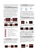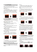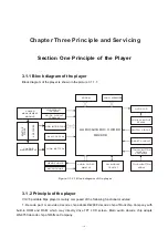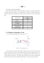
Figure 3.2.3.1 Flash circuit schematic diagram
2. Working principle: Flash Memory is the storage unit of the player and all AV and image files must
be stored in FLASH. Flash module is composed of two groups of FLASH chip K9G8G08U0M with the
specification 2G (H model is 4G). Flash chip and main decode RK2608 are connected through 8 data
lines to complete the read, write and delete of inside files. VCC provides 3.3V voltage for FLASH
working. R35, R36 are pull-up resistor of /CE and R40 is pull-down resistor of /WP. VCC is power supply
pin of FLASH. /CE is chip-selection signal, effective when in high level. VCC supplies 3.3V voltage and
FLASH begins working. /RE, /WE are read-effective and write-ettective signal ports to control rear and
write function of FLASH. I/O1
I/O8 are 8 data lines to fulfill the exchange of FLASH and outside data to
realize the function of write, delete and edit of Mp3.
D2
FREN
FALE/RS/A1
FCE0
D3
D6
FCLE/A2
D5
D4
D7
D1
FWEN
D0
RD/BY
D_GND
D_GND
R32
0R
FCE1
R35
47K
C40
104
R36
47K
C39
104
FWP
R40
47K
R37
10K
U4
NAND FLASH
RES#
1
NC
2
NC
3
NC
4
NC
5
R/B2
6
R/B1
7
RE
8
CE1
9
CE2
10
NC
11
VCC
12
VSS
13
NC
14
NC
15
CLE
16
ALE
17
WE
18
WP
19
NC
20
NC
21
NC
22
NC
23
NC
24
NC
25
NC
26
NC
27
NC
28
I/O0
29
I/O1
30
I/O2
31
I/O3
32
NC
33
NC
34
NC
35
VSS
36
VCC
37
PRE
38
NC
39
NC
40
I/O4
41
I/O5
42
I/O6
43
I/O7
44
NC
45
NC
46
NC
47
NC
48
VCC
GND
VCC
VCC
When machine is in FM state, FM digital audio signals input from INPUT pin (pin 27, 28) of
WM8750, after digital filtering and echo processing inside WM8750, and then output to headphone jack
directly.
3.2.3 FLASH circuit
1. FLASH circuit schematic diagram is shown in the figure 3.2.3.1:
- 19 -

