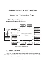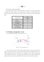
Figure 3.2.12.2 1.8V power circuit diagram
EN
C98
101
U6
TPS62200/FAN5307* SOT23-5
VI
1
GND
2
EN
3
FB
4
SW
5
C45
106/X5R
P_GND
P_GND
VDD
R45
10k
L13
CDRH3D16-100
R44
390K 1%
C44
47PF
VDD
R42
240K 1%
V_ADJ
2
D_GND
D_GND
C48
106/X5R
R43
100K 1%
Q8
MMST3904
D_GND
R46
47k
VDD
2. Working principle: seen from the circuit diagram, 3.3V power is supplied by IC TPS79333 and
peripheral circuit. TPS79333 is a linear volatge stabilizing module (also called as LDO) and its EN pin is
the enable pin that controls normal working, effective when in high level; BYPASS pin has a resistor
inside, which may constitute low-pass filter together with external 103 capacitor C4 to decrease output
noise.
1.8V power of the player’s working is supplied by TPS62200 and peripheral circuit. TPS62200 is
high-efficience voltage drop DC-DC convertor and EN pin is enable pin, effective when in high. The
relationship between TPS62200 output voltage and FB pin feedback resistance is:
From the above, output voltage is about 1.75V.
3.2.13 Reset circuit
1. Reset circuit supplies reset signals for the player. Reset circuit diagram is shown in the picture
3.2.13.1:
VOUT=0.5
( )
1+
R42
R43
Figure 3.2.13.1 Reset circuit diagram
GND
R56
0R
RESETN
C23
104
Q3
SS8050LT
R21
220K
R22
1M
C19
104
R20
10K
VCC
- 27 -


