2. Working principle: when the player power on, voltage stabilizing circuit begins to work and 3.3V
voltage VCC outputs. Voltage on two sends of capacitor C19 cannot change suddenly, so B electrode of
triode Q3 is low level, Q3 is in cutoff state, RESETN is high level to reset for Rk2608 and display screen.
Meanwhile, VCC charges capacitor C19. When B electrode voltage of Q3 reaches connected voltage,
Q3 is on, VCC is on to ground, RESETN becomes low level and reset of the player finishes. Reset time
is decided by C19 and parameters of resistor R21 and R22.
3.2.14 Power on/off control circuit
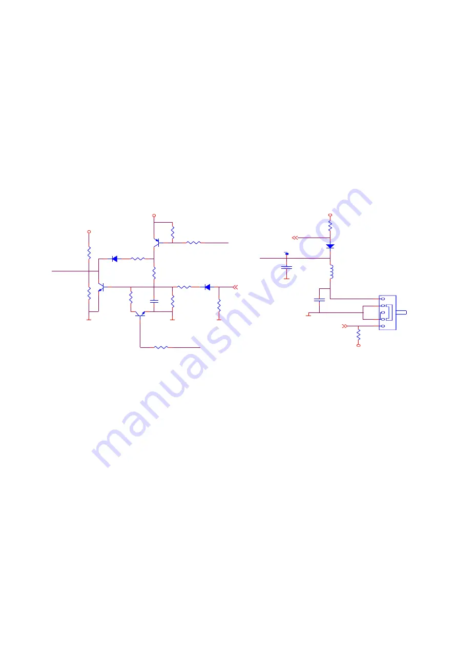
1. Power on/off control circuit diagram is shown in the picture 3.2.14.1:
Figure 3.2.14.1 Power on/off control circuit diagram
2. Working principle: START/PLAY/PAUSE is a group of combination buttons and functions are
different in different working times, decided by software. When the player is in power-off state without
connecting with USB, Q4 is in cutoff state. When power-on button Sw1 is in ON position, START is
pulled down to ground to output low level, Q4 is on, diode D8 is also on, BATT pulls EN up through Q4
and D8, TPS62200 and TPS79333 begin to enter working state to output 1.75V and 3.3V voltage to
suppl power for the entire system. System voltage VCC, VDD and OLED (13V) begin to output, crystal
oscillator Y1 oscillates, reset circuit works, main chip and display screen initialize, OSD appears and
machine begins to work.
When in power-on state, press START/PLAY/PAUSE, Q4 is on and BATT produces a voltage drop
through CE electrode of Q4. Because VCC voltage is normal, the circuit composed through R92, R93,
C87 makes N electrode of D12 keeps 3.3V voltage. D12 cannot be on and it in cutoff state, but after
pressing button, voltage of PLAY/PAUSE pin changes and then inputs to pin 57 of Rk2608 to realize
different functions in different operation interfaces.
SFI0402-050E100NP
C85
VCC
P_GND
PLAY/PAUSE
2
SW1
1
4
2
3
START
R58
47K
D_GND
HOLD
VCC
L22
601 DCR<350m¦¸
D9
1N4148WS
R85
100k
C86
SFI0402-050E100NP
PLAY
R65
10K
P_GND
Q4
MMST3906
R92
330K
C87
475/X5R
Q5
SS8050LT
R96
2.7M
Q7
SS8050LT
D12
1N4148WS
R95
47K
R94
100K
R87
330K
R88
1M
D8
1N4148WS
R93
10M
R89
10K
R90
10K
BATT
P_GND
VCC
P_GND
OFF
EN
START
R97
1M
START
- 28 -


