- -
43
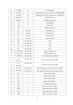
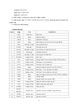
3. PIN Description
SYMBOL
TYPE
DESCRIPTION
CLK
Clock
The system clock input. All other inputs are registered to the SDRAM on the
rising edge of CLK
CKE
Clock Enable
Controls internal clock signal and when deactivated, the SDRAM will be one
of the states among power down, suspend or self refresh
CS
Chip Select
Enables or disables all inputs except CLK, CKE, UDQM and LDQM
BA0, BA1
Bank Address
Selects bank to be activated during RAS activity Selects bank to be
read/written during CAS activity
A0 ~ A11
Address
Row Address : RA0 ~ RA11, Column Address : CA0 ~ CA7 Auto-precharge
flag : A10
RAS, CAS, WE
Row Address Strobe, Column
Address Strobe, Write Enable
RAS, CAS and WE define the operation Refer function truth table for details
UDQM, LDQM
Data Input/Output Mask
Controls output buffers in read mode and masks input data in write mode
DQ0 ~ DQ15
Data Input/Output
Multiplexed data input / output pin
VDD/VSS
Power Supply/Ground
Power supply for internal circuits and input buffers
VDDQ/VSSQ
Data Output Power/Ground
Power supply for output buffers
NC
No Connection
No connection
3.5.2 Function introduction to RK2608
1. Features
◆
128 pins LQFP package
◆
Typical power voltage 3.3V(IO), 1.8V(Core)
◆
Use one 24MHz crystal oscillator
◆
38 GPIO (8bits P0,P1,P3,14bits P2)
◆
10-bit low resolution ADC with 4-channel Analog Input
◆
Build in Stereo 24-bit Delta-Sigma DAC with on-chip headphone amplifier
◆
Build in Stereo 16-bit Sigma-Delta ADC (Line-in /FM Input/ Microphone with analog mixer)
◆
40 levels digital volume control
◆
Support external CODEC through I2DSP interface
◆
Support I2C interface
◆
Support USB 2.0 high speed and full speed
◆
Integrated 3 Channel DMA
◆
Embedded DSP Core:
·
4K words Boot Sync ROM


